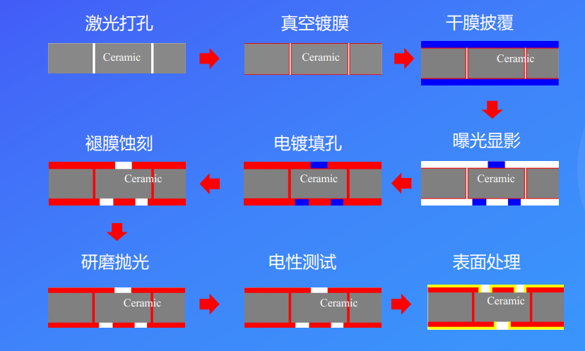
Making Process Of DPC Ceramic PCB
DPC technology in Ceramic PCB manufacturing process is the same as FR4 PCB, except the substrate is the ceramic and it is fragile and easy to be broken. The manufacturing process of DPC ceramic PCBs typically involves the following steps:
1. Material Selection: The first step is to select the appropriate materials for the ceramic substrate and the copper conductors. The ceramic substrate material for DPC technology is typically aluminum oxide (Al2O3) or aluminum nitride (ALN), which have high thermal conductivity and good electrical insulation properties. (ZrO2 and Si3N4 also is available, but they are rarely to use in DPC ceramic substrate.) Copper is used as the conductor material because of its high conductivity.
2. Substrate Preparation: In generally, the substrate is in a big size and need to be cut into a required dimension by laser cutting method. It is worth noting that the laser energy is difficult to set, if the energy is too high then the cut edge substrate will be black, and the substrate cannot be cut well if the energy is low, so choosing a manufacturer who has rich experience is important. The ceramic substrate is cleaned and polished to achieve a smooth surface.
3. Drill hole: The drilling process is to drill the plated through hole (PTH)and non-plated through holes (NPTH) as PCB drawing is required to allow for component placement and connection. The minimum hole diameter we can make is 4mil, which is 0.1mm.
4. Metallization/sputtering: A thin layer of metal, usually molybdenum or tungsten, is deposited on the ceramic substrate using a sputtering process. This layer acts as an adhesive layer for the subsequent copper layers.
5. Copper Foil Deposition: A thin layer of copper foil is deposited onto the ceramic substrate using a high-temperature adhesive. This process is repeated multiple times to achieve the desired thickness of the copper conductors. This step is also known as PVD or vacuum plating.
6. Dry film: This process is similar to PCB manufacturing. Apply dry film onto the thin copper film on both sides of the copper plated ceramic substrate. And the copper layer is then patterned into various shapes and traces by using a photolithography process.
7. Exposure: A photo-sensitive film, similar to a photographic film and distinct from thin or thick films, is created using traditional photomask technology. Firstly, the flat photomask is meticulously aligned and affixed onto the dry film layer positioned atop a ceramic substrate. The composite structure is then transported to an exposing chamber where a vacuum is established to ensure uniform and consistent exposure. Once the desired vacuum level is achieved, ultraviolet (UV) light is projected through the photomask onto the dry film, initiating polymerization upon contact with the photoresist. In contrast, the areas of dry film not exposed to UV radiation remain unaltered and retain their original chemical composition.
8. Copper plating: The initial step involves plating the copper leads, followed by depositing copper to fill the dry film's exposed parts on the ceramic substrate through plating technology, creating the copper features with a suitable thickness and width we need. This process results in a metallized circuit area with smooth, flat, and slender characteristics, providing efficient heat dissipation. However, in cases where the plated copper exceeds the desired thickness, the excess copper can be eliminated by utilizing a high-end ceramic grinding machine with 1μm precision per grinding cycle, similar to the one used in the Via-in-Pad process.
9. Strip and etch: Stripping the dry film and then etching. The purpose of etching is to remove the unexposed area, where we do not need circuits on.

10. Polish: The purpose of polishing process is to make the ceramic surface more flat and if the copper plating is a little bit thicker than required, polishing can remove a little copper make it is in conform to drawing.
11. E-test: The finished DPC ceramic PCBs are tested for electrical continuity and insulation resistance to ensure their quality.
12. Surface treatment: The same as FR4 PCB, coating a layer of surface finishing can protect the circuit from oxidation and improve the corrosion of the ceramic PCB. In generally, the surface finishings for DPC technology are OSP, ENIG and ENEPIG. ENEPIG is the best solution for wire bonding process.
Overall, the manufacturing process of DPC ceramic PCBs requires precise control and careful handling to achieve a high-quality product that can withstand the extreme conditions of high-temperature applications.


 HOME
HOME


