


 HOME
HOME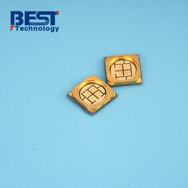
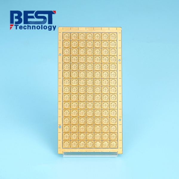
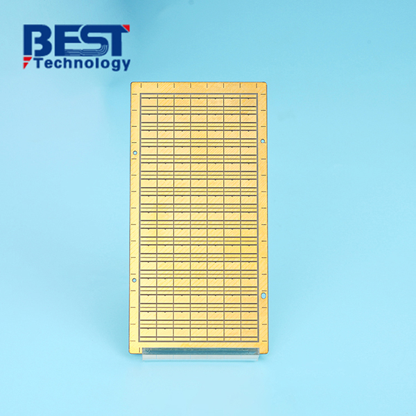
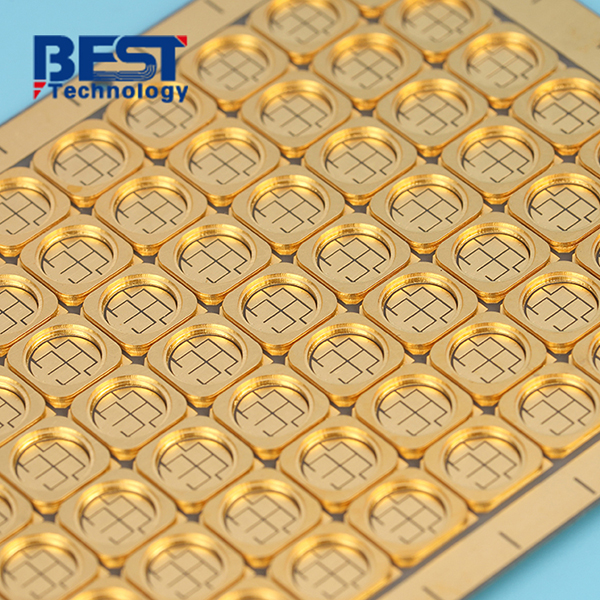
Tiny Size DBC Ceramic Substrate PCB For Scientific Education


Board Thickness: 2.0mm+/-10%
Conductor: 300um AgPd
Solder Mask: N/A
Silkscreen: N/A
Surface Finishing: ENIG 1u"
Application: Scientific Education
| Item1 | DCB/DBC Capabilities | |||||
|---|---|---|---|---|---|---|
|
Layer Count |
1-2 Layers |
|||||
|
Max Board Dimension |
120mmx180mm |
|||||
|
Min Board Thickness |
0.254mm |
|||||
|
Max Board Thickness |
2.0mm |
|||||
|
Conductor Thickness |
100-600μm |
|||||
|
Min Line Width/Line Space |
300/300μm |
|||||
|
Substrate Type |
AI2O3 |
|||||
|
Substrate Thickness |
0.254-2.0mm |
|||||
|
Min Hole Diameter |
0.25mm (No Via Hole) |
|||||
|
Min Hole Spacing |
250μm |
|||||
|
Min PAD Ring(Single) |
0.125mm |
|||||
|
PTH Wall Thickness |
N/A |
|||||
|
Min Solder PAD Dia |
0.5mm |
|||||
|
Min Soldermask Bridge |
Green Oil 130μm; Others 150μm |
|||||
|
Min BAG PAD Margin |
0.35mm |
|||||
|
PTH/NPTH Dia Tolerance |
0.075mm |
|||||
|
Hole Position Deviation |
75μm |
|||||
|
Outline Tolerance |
Laser: +/-0.13mm |
|||||
|
Line Width/Spac Tolerance |
±20% |
|||||
|
Surface Treatment |
OSP/Immersion Gold/Nickel Plated Gold/Immersion Silver/Nickel Plated |
|||||
|
Thermal Stress |
7.3ppm/k |
|||||
| Item2 | Attribute | ||
|---|---|---|---|
|
Brand |
CeramTec / GTT / Huaqing / Laird / Maruwa / Rogers / Toshiba |
||
|
Base Material |
AI2O3 |
||
|
Base Material Thickness (exclude conductor) |
0.45-3.2mm |
||
|
Thermal Conductivity |
24-170W/mk |
||
|
Soldermask Type |
Aluminum Oxide |
||
|
Tg Value |
800℃ |
||
|
Halogen Free |
No |
||
|
Breakdown Voltage |
>15KV/mm |
||
|
Dielectric Constant (MHZ) |
9.4 (1MHz); 9.1 (13GHz) |
||
|
Water Absorption |
≤0.5% |
||
|
ROHS |
Yes |
||
|
Flammability |
Grade A |
||
|
Thermal Conductivity (W/m.K, or W/m.C) |
24-170W/mk |
||
|
Dielectric Strength |
15KV/mm |
||
|
Wrap & Twist |
3% |
||
| Prototype(<1m²) | Layers | Normal Service | Expedited Service |
|---|---|---|---|
|
DCB/DBC Ceramic PCB |
1 Layer |
2 - 3 weeks |
1.5 weeks |
|
2 Layers |
2 - 3 weeks |
1.5 weeks |
| Production | Layers | Normal Service | Expedited service |
|---|---|---|---|
|
DCB/DBC Ceramic PCB |
1 Layer |
3 - 4 weeks |
1.5 - 2 weeks |
|
2 Layers |
3 - 4 weeks |
1.5 - 2 weeks |

DBC (Direct Bonding Copper) is a technology that bonds the copper conductor on the ceramic substrate directly under an appropriate temperature. The binding force between the pure copper and the ceramic substrate is very reliable.
1. Material: Aluminum Nitride/Aluminum Oxide/ZrO2
2. Function: Heat dissipation ceramics and electrical insulation.
3. Type: Metallized ceramic.
4. Custom service available.

Background:
Bioly Electronics is a company that specializes in developing innovative technologies for the life sciences industry. They are planning to design a new electrochemical biosensor for a research project, and they have decided to use a ceramic PCB as the base plate for the biosensor.
At the initial step in the design process was to select the appropriate substrate material for the biosensor. After considering various options, Bioly Electronics chose a double-sided DBC ceramic PCB due to its excellent electrical insulation and high thermal conductivity. The ceramic substrate provides a stable and reliable platform for the biosensor to function on.
Project Challenge:
- The copper thickness required 300um, it is not easy to plate such thick copper in one time.
- The copper surface should have good flatness, it is difficult to control especially copper needs to be plated multiple times to achieve 300um.
- It is a big challengeA to protect the copper surface from scratch during the complex manufacturing process.
DBC ceramic PCB for Biosensor application:
An electrochemical biosensor is a device that detects biological or chemical species by converting the biochemical reaction into an electrical signal. A Double-Sided DBC Ceramic Circuit Board was used as the substrate for the biosensor due to its good performance. The biosensor was fabricated by depositing a metal layer onto the substrate and immobilizing the biorecognition element on the metal surface using a biofunctionalization process. This process involved the covalent attachment of the biorecognition molecules to the metal surface, which allowed for the specific detection of the target analyte. The DBC ceramic substrate provided excellent electrical insulation and high thermal conductivity, which were critical for the biosensor's performance. After testing, the biosensor exhibited high sensitivity and selectivity, indicating that it was well-suited for its intended application.
Results and Benefits:
Customer was satisfied to our hard work because the ceramic board performed excellent when mounted into the biosensor, makes it is well-suited for the end application. Now we are the only one ceramic board long-established supplier of Bioly in China, and we fabricate more than 10,000 pieces such board for them every month.

 Products
 About us
 Contact us


