


 HOME
HOME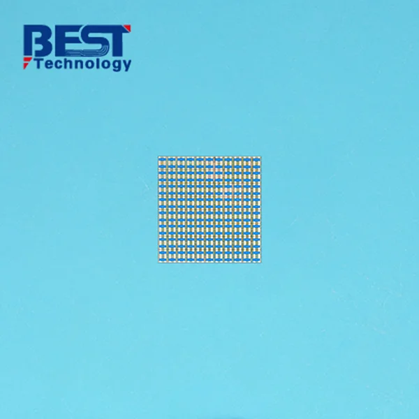
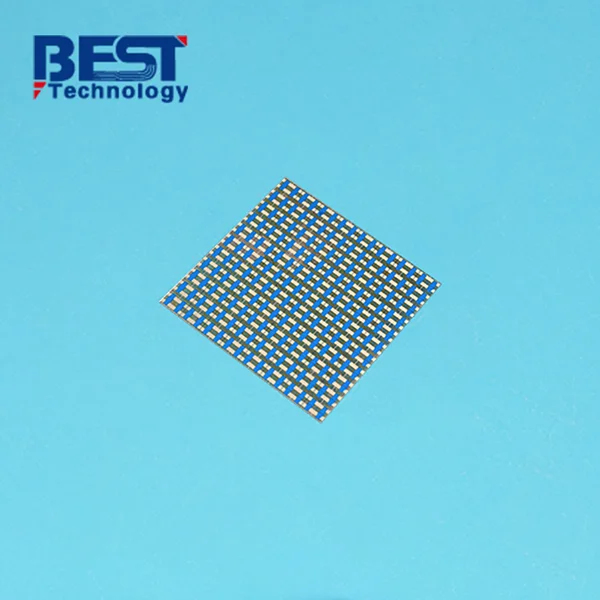
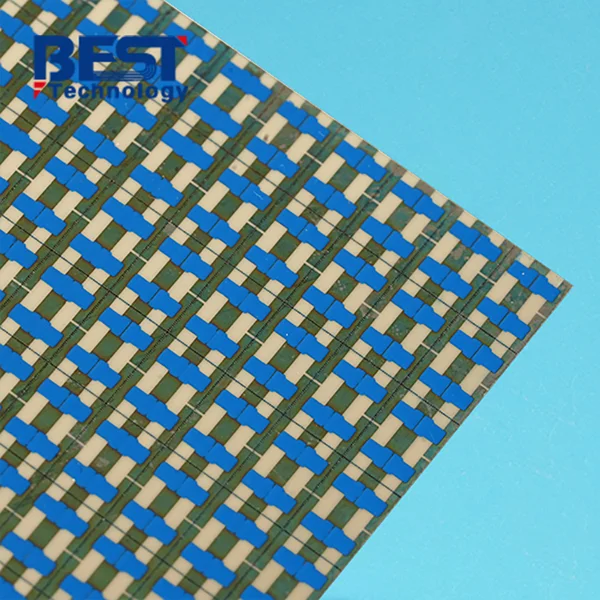
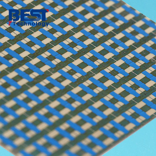
Soul Ultra-thin Film Ceramic PCB Design For Robot Control System


Board Thickness: 1.0mm
Conductor: 0.1umTi+0.2umPt
Solder Mask: N/A
Silkscreen: N/A
Surface Finishing: N/A
Application: Robot Control System
| Item1 | Thin Film Capabilities | Special Needs |
| Circuit layers | 1~2 Layers | N/A |
| Product Unit Size | 0.5mmx0.5mm-200mmx200mm | 0.25mmx0.25mm |
| Substrate Thickness Tolerance | ≤ ± 10% | ±0.02mm |
| Element Size Tolerance | ±0.05mm | ±0.03mm |
| Minimum Line Width@Thickness<3μm | 20μm | 10μm |
| Line Width Accuracy | ±5μm | ±2μm |
| Forecast Minimum Size Of Gold-tin Solder | 100μm*100μm | 50μm*50μm |
| Distance From Wire To Substrate Edge | 50μm | min 20μm |
| Minimum Land Size Around Vias | ≥Aperture+50μm | N/A |
| Front, Back, Multilayer Alignment Accuracy | ≤ ± 5μm | ± 1μm |
| Front, Side Alignment Accuracy | ≤ 20μm | N/A |
| Available Cutter Width | 0.1, 0.15, 0.2mm | N/A |
| Cutting Accuracy Of Grinding Wheel | ± 50μm | ± 20μm |
| Laser Cutting Precision | ± 20μm | N/A |
| Minimum Hole Diameter | 0.5*Board Thickness | N/A |
| Aperture Tolerance | ± 10% | N/A |
| Solid Hole Diameter | 0.075, 0.1mm | N/A |
| Item2 | Attributes | Special Needs |
| Brand | BSTCeramicPCB | N/A |
| Substrate type | AlN, Al2O3, Si, Quartz, Glass-ceramic, Diamond, Sapphire | N/A |
| Substrate Roughness (Ra) | ≤0.1μm | ≤0.05μm |
| Coating Type | Metal film, resistive film, dielectric film, functional film, etc. | N/A |
| Film Thickness Tolerance | ±20% | ±5% |
| Resistive film square resistance | 10-200 | N/A |
| Resistance value accuracy (laser trimmable) | ±0.1% | ±0.05% |
| Resistance value accuracy (no laser trimming) | ±5% | ±3% |
| Temperature coefficient of resistance | ±25ppm | min±10ppm |
| Rapid Prototype | Layer | Normal Delivery | Expedited Service |
| Thin Film Ceramic PCB | 1 | 3-4.5 Weeks | 2-2.5 Weeks |
| 2 | 4-6 Weeks | 2-2.5 Weeks |
| Mass Production | Layer | Normal Delivery | Expedited Service |
| Thin Film Ceramic PCB | 1 | 4-5 Weeks | 2-3 Weeks |
| 2 | 4-6 Weeks | 2-3 Weeks |
Thin film ceramic boards are thin, lightweight, and made of ceramic materials like alumina or aluminum nitride. They have high thermal conductivity, excellent electrical insulation, and low loss tangent. These boards are suitable for high-frequency applications, chemically resistant, and offer precision and stability. They can integrate semiconductor components and provide hermetic packaging for sensitive electronics.
Benefits of thin film ceramic PCB
- Small size and fine traces
- Low loss tangent
- High-frequency performance
- Precision and stability
- Integration with semiconductor components
- Hermetic package
- Chemical and corrosion resistance
Customer background:
AutoLine Robotics Corporation specializing in industrial automation solutions and robotic systems for manufacturing and assembly processes. With a focus on efficiency and precision, AutoLine delivers advanced automation solutions to optimize manufacturing operations.
Customer Project Requirements:
Their R&D team was tasked with developing an automated inspection and sorting system for a large-scale manufacturing plant. The project demanded high-precision control systems and sensors for reliable product inspection and sorting in real-time. To meet the precision requirements for the automated inspection and sorting system, AutoLine sought high-performance Thin Film Ceramic PCBs for their control systems and sensors.
Project challenge:
The only challenge was to achieve extremely fine circuit patterns with low dielectric losses to ensure precise signal integrity and accurate data processing. The circuit boards needed to demonstrate high reliability and stability to withstand continuous operation in industrial environments.
Post-Project Outcome:
After receiving the demands of AutoLine, our engineering team draw the layout and circuit design according to their requirements. After getting their approval, we made the samples within 1.5weeks and delivered them out immediately. After install and test the electrics, Autoline Robotics expressed utmost satisfaction with the remarkable performance and reliability of the Thin Film Ceramic PCBs. The successful integration of these advanced circuit boards within their automated inspection and sorting system elevated manufacturing efficiency for their valued clients. Notably, this partnership enabled AutoLine Robotics to expand its range of industrial automation solutions, drawing the attention of new clients in search of advanced and dependable robotics systems.

 Products
 About us
 Contact us


