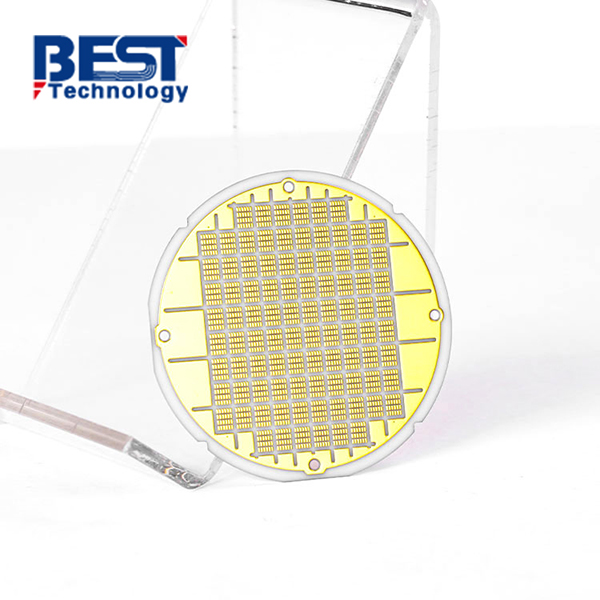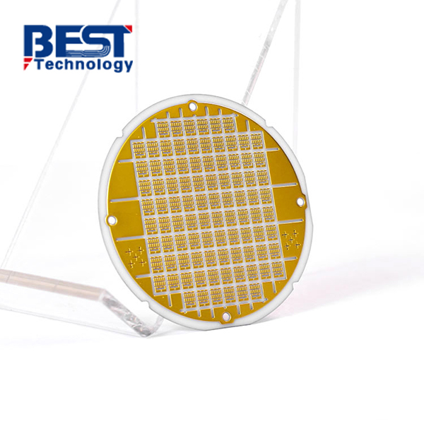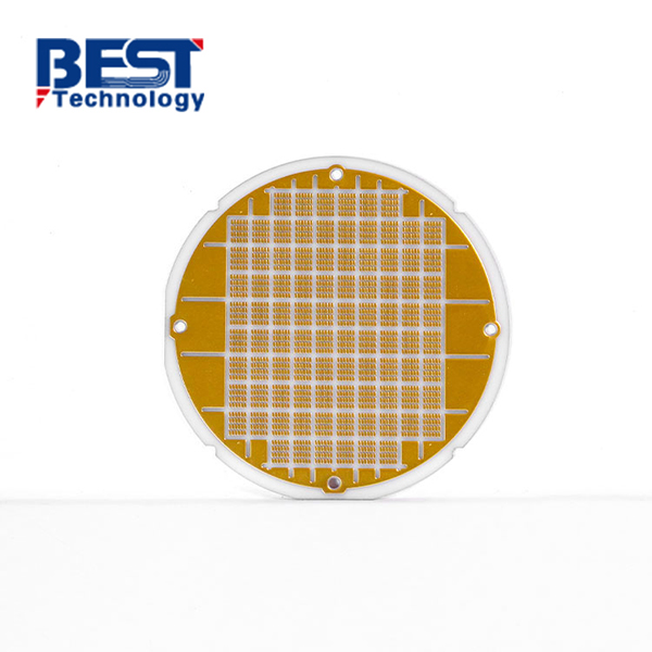
DPC Al2O3 Ceramic Substrate Circuit Board For Cooler


Board thickness: 0.38mm+/-0.1mm
Conductor: 35um copper, 200um copper in specific area
Solder mask: N/A
Silkscreen: N/A
Surface finishing: ENEPIG 3u’’
Application: Cooler
| Item1 | DPC Capabilities | |||||
|---|---|---|---|---|---|---|
|
Layer Count |
1-2 Layers |
|||||
|
Max Board Dimension |
120mmx180mm | |||||
|
Min Board Thickness |
0.15mm |
|||||
|
Max Board Thickness |
6.0mm |
|||||
|
Conductor Thickness |
50/50μm |
|||||
|
Min Line Width/Line Space |
3/3mil (0.075/0.075mm) |
|||||
|
Substrate Type |
AI2O3, ALN, Si3N4 |
|||||
|
Substrate Thickness |
0.15-6mm |
|||||
|
Min Hole Diameter |
100μm |
|||||
|
Min Hole Spacing |
250μm |
|||||
|
Min PAD Ring(Single) |
0.125mm |
|||||
|
PTH Wall Thickness |
8um |
|||||
|
Min Solder PAD Dia |
0.25mm |
|||||
|
Min Soldermask Bridge |
Green Oil 130μm; Others 150μm |
|||||
|
Min BAG PAD Margin |
0.3mm |
|||||
|
PTH/NPTH Dia Tolerance |
0.05/0.075mm |
|||||
|
Hole Position Deviation |
50-75μm |
|||||
|
Outline Tolerance |
Laser: +/-0.13mm |
|||||
|
Line Width/Spac Tolerance |
±20% |
|||||
|
Surface Treatment |
OSP/Immersion Gold/Nickel Plated Gold/Immersion Silver/Nickel Plated |
|||||
|
Thermal Stress |
7.3pmm/k |
|||||
| Item2 | Attribute | ||
|---|---|---|---|
|
Brand |
CeramTec / GTT / Huaqing / Laird / Maruwa / Rogers / Toshiba |
||
|
Base Material |
AI2O3 |
||
|
Base Material Thickness (exclude conductor) |
0.15-6mm |
||
|
Thermal Conductivity |
24-170W/mk |
||
|
Soldermask Type |
Aluminum Oxide |
||
|
Tg Value |
800℃ |
||
|
Halogen Free |
No |
||
|
Breakdown Voltage |
15 KV/mm |
||
|
Dielectric Constant (MHZ) |
9.4 (1MHz); 9.1 (13GHz) |
||
|
Water Absorption |
≤0.5% |
||
|
ROHS |
Yes |
||
|
Flammability |
Grade A |
||
|
Thermal Conductivity (W/m.K, or W/m.C) |
24-170 W/mk |
||
|
Dielectric Strength |
>15 KV/mm |
||
|
Wrap & Twist |
3% |
||
| Prototype(<1m²) | Layers | Normal Service | Expedited Service |
|---|---|---|---|
|
DPC Ceramic PCB |
1 Layer |
DPC: 2 - 3 weeks |
DPC: 1.5 weeks |
|
2 Layers |
DPC: 2 - 3 weeks |
DPC: 1.5 weeks |
| Production | Layers | Normal Service | Expedited service |
|---|---|---|---|
|
DPC Ceramic PCB |
1 Layer |
DPC: 3 - 4 weeks |
DPC: 1.5 - 2 weeks |
|
2 Layers |
DPC: 3 - 4 weeks |
DPC: 1.5 - 2 weeks |
Best Technology: Leading DPC Ceramic PCB Manufacturer
Best Technology is a premier manufacturer in the ceramic PCB industry, renowned for their commitment to excellence and customizable solutions. Here's why they stand out:
- Expertise and Technical Know-How: With highly skilled engineers and technicians, Best Technology offers extensive expertise and stays ahead of industry trends to provide innovative solutions.
- Comprehensive Design Support: Best Technology provides comprehensive design support, collaborating closely with clients on FPC design optimization, material selection, and manufacturability to ensure high-quality and high-performance outcomes.
- Prototyping and Fast Turnaround: They offer rapid prototyping services and fast turnaround times, allowing customers to validate designs quickly and meet tight project deadlines.
- Superior Quality and Reliability: Best Technology prioritizes quality control, utilizing advanced testing equipment and rigorous inspection procedures to deliver superior, reliable DPC ceramic PCBs that exceed customer expectations.
DPC ceramic PCB specification:
|
Substrate material: |
96% Al2O3 |
|
Board thickness: |
0.38mm+/-0.1mm |
|
Conductor: |
35um copper, 200um copper in specific area |
|
Solder mask: |
N/A |
|
Silkscreen: |
N/A |
|
Surface finishing: |
ENEPIG 3u’’ |
|
Application: |
Cooler |
Background:
OptoTech is a company of VSCEL laser technologies, specializing in high-performance VSCEL lasers. They cater to various industries such as telecommunications, medical devices, and scientific research. OptoTech Solutions is facing challenges with the thermal management and electrical performance of their VSCEL lasers, which are crucial for maintaining laser stability and efficiency. They are seeking a reliable ceramic PCB supplier that can provide high-quality ceramic circuits for their VSCEL laser systems.
PCB challenge:
- The ceramic PCB needs a very good flatness to perform good thermal management for their VECEL lasers.
- The whole board is covered by copper, it is not easy to protect from oxidation and scratch.
- Some specific areas required 200um copper, so it needs to proceed plating process several times to achieve the required thickness, which will affect the surface flatness.
- The customer wants to add solder paste on the pads for 1mm, it is difficult to control the thickness, especially since the copper thickness is different on some pads.
Solution:
During the second plating, we protected the copper surface so that no need to add extra copper by film, all the operators paid high attention during the whole process, and finally we finished the products and applied the solder paste successfully by a stepped stencil.
Result and Benefits:
The customer appreciated our hard work and dedicated work attitude, they gave us a big thump up and sent some other similar projects to us. Now we are still in cooperating new project.


 HOME
HOME


