


 HOME
HOME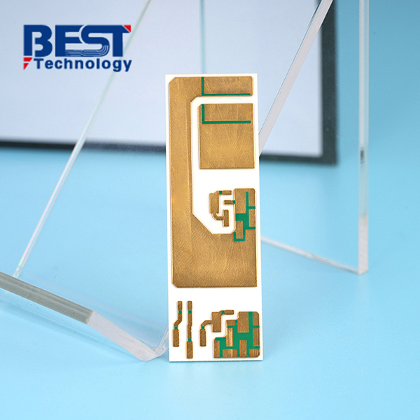
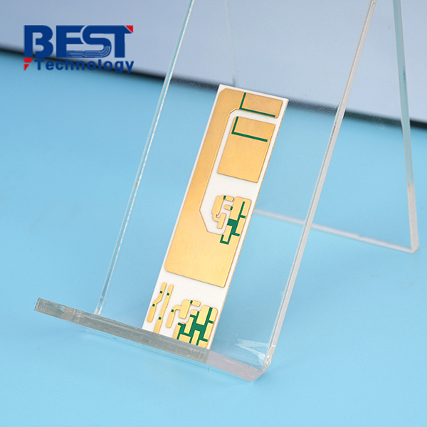
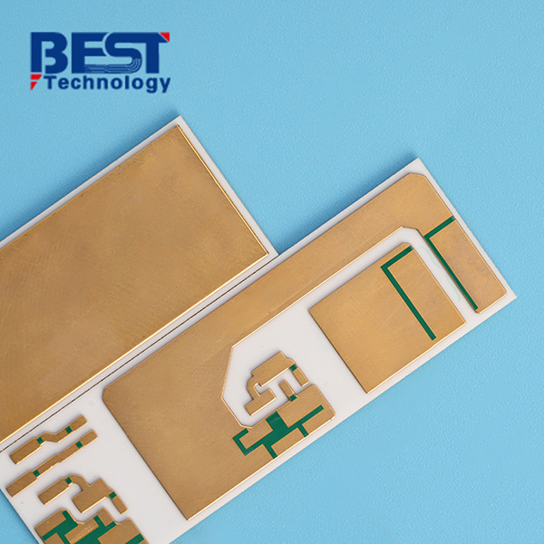
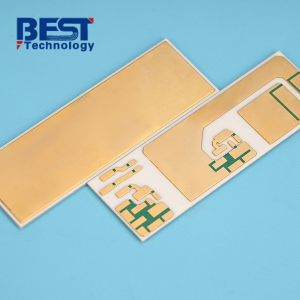
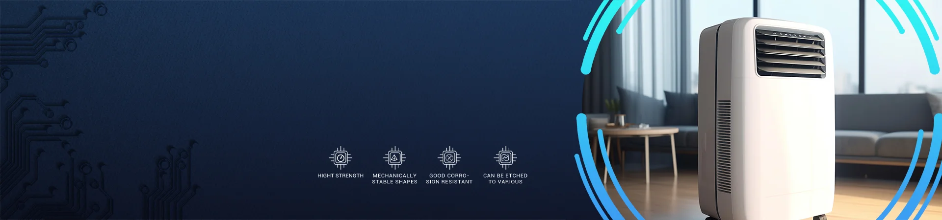
Custom Wholesale Double-sided Nickel-palladium-gold DBC Ceramic PCB For Automotive Systems


Board Thickness: 0.635mm+/-0.1mm
Conductor: 100um copper
Solder Mask: Green Glass Glaze
Silkscreen: N/A
Surface Finishing: ENEPIG 3u’’
Application: Microfluidic devices
| Item1 | DCB/DBC Capabilities | |||||
|---|---|---|---|---|---|---|
|
Layer Count |
1-2 Layers |
|||||
|
Max Board Dimension |
120mmx180mm |
|||||
|
Min Board Thickness |
0.254mm |
|||||
|
Max Board Thickness |
2.0mm |
|||||
|
Conductor Thickness |
100-600μm |
|||||
|
Min Line Width/Line Space |
300/300μm |
|||||
|
Substrate Type |
AI2O3 |
|||||
|
Substrate Thickness |
0.254-2.0mm |
|||||
|
Min Hole Diameter |
0.25mm (No Via Hole) |
|||||
|
Min Hole Spacing |
250μm |
|||||
|
Min PAD Ring(Single) |
0.125mm |
|||||
|
PTH Wall Thickness |
N/A |
|||||
|
Min Solder PAD Dia |
0.5mm |
|||||
|
Min Soldermask Bridge |
Green Oil 130μm; Others 150μm |
|||||
|
Min BAG PAD Margin |
0.35mm |
|||||
|
PTH/NPTH Dia Tolerance |
0.075mm |
|||||
|
Hole Position Deviation |
75μm |
|||||
|
Outline Tolerance |
Laser: +/-0.13mm |
|||||
|
Line Width/Spac Tolerance |
±20% |
|||||
|
Surface Treatment |
OSP/Immersion Gold/Nickel Plated Gold/Immersion Silver/Nickel Plated |
|||||
|
Thermal Stress |
7.3ppm/k |
|||||
| Item2 | Attribute | ||
|---|---|---|---|
|
Brand |
CeramTec / GTT / Huaqing / Laird / Maruwa / Rogers / Toshiba |
||
|
Base Material |
AI2O3 |
||
|
Base Material Thickness (exclude conductor) |
0.45-3.2mm |
||
|
Thermal Conductivity |
24-170W/mk |
||
|
Soldermask Type |
Aluminum Oxide |
||
|
Tg Value |
800℃ |
||
|
Halogen Free |
No |
||
|
Breakdown Voltage |
>15KV/mm |
||
|
Dielectric Constant (MHZ) |
9.4 (1MHz); 9.1 (13GHz) |
||
|
Water Absorption |
≤0.5% |
||
|
ROHS |
Yes |
||
|
Flammability |
Grade A |
||
|
Thermal Conductivity (W/m.K, or W/m.C) |
24-170W/mk |
||
|
Dielectric Strength |
15KV/mm |
||
|
Wrap & Twist |
3% |
||
| Prototype(<1m²) | Layers | Normal Service | Expedited Service |
|---|---|---|---|
|
DCB/DBC Ceramic PCB |
1 Layer |
2 - 3 weeks |
1.5 weeks |
|
2 Layers |
2 - 3 weeks |
1.5 weeks |
| Production | Layers | Normal Service | Expedited service |
|---|---|---|---|
|
DCB/DBC Ceramic PCB |
1 Layer |
3 - 4 weeks |
1.5 - 2 weeks |
|
2 Layers |
3 - 4 weeks |
1.5 - 2 weeks |
The DCB Ceramic PCB, featuring a super-thin substrate, offers exceptional electrical isolation, high thermal conductivity, excellent solderability, and strong bonding strength. It shares similarities with normal FR4 PCBs in terms of being etchable, but its distinguishing feature lies in its remarkable ability to handle high current loads. Consequently, the DCB Ceramic PCB has emerged as the go-to material for constructing and interconnecting high-power semiconductor electronic circuits. Moreover, it has paved the way for the future packaging trend known as "Chip On Board" (COB) technology, which leverages the advantages of the DCB Ceramic PCB as its foundation.
DBC ceramic PCB specification:
|
Substrate material: |
96% Al2O3 |
|
Board thickness: |
0.635mm+/-0.1mm |
|
Conductor: |
100um copper |
|
Solder mask: |
Green Glass Glaze |
|
Silkscreen: |
N/A |
|
Surface finishing: |
ENEPIG 3u’’ |
|
Application: |
Automotive Systems |
 High -Power Semiconductor
 Solar Panel
 Aerospace
 Automobile Product
 Communications Industry
 High Power LED Lighting
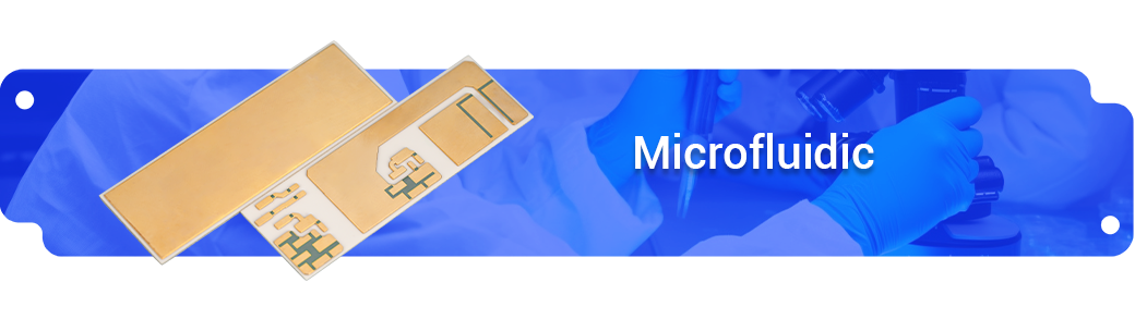
Background:
Mellenklu is a startup company that aims to design and develop a microfluidic device for drug delivery applications. The company's research and development team has decided to use a single sided DBC (Direct Bonded Copper) ceramic PCB as the substrate for their microfluidic device.
The microfluidic device will be designed to have multiple channels and valves to enable precise control of fluid flow. The single sided DBC ceramic PCB will be used as the base material due to its excellent thermal conductivity, high mechanical strength, and low coefficient of thermal expansion. And DBC ceramic PCB acts as the conductive pathway for the microfluidic device. The copper layer will be patterned to create the channels and valves needed for the device.
Project Challenge:
- The ceramic circuit board requires ship by panel and each panel has 24 slots in it, it is difficult to control the laser energy when drill the slot.
- The AlN ceramic substrate is fragile and easy to be broken during production run, so we need to be more carefully.
DBC Ceramic PCB For Microfluidic Application:
Microfluidic devices are used to manipulate and analyze small volumes of fluids. A Single-Sided DBC Ceramic Circuit Board was used as the substrate for a microfluidic device designed for drug discovery. The microfluidic device was fabricated by creating microchannels on the ceramic substrate using photolithography and sintering. The metal layers on the substrate were used as electrodes to manipulate the fluids and perform electrochemical measurements. Mellenklu's team will assemble the microfluidic device by bonding the single sided DBC ceramic PCB to a cover layer using an adhesive or a thermal bonding process. The cover layer will be made of a transparent material such as glass or plastic to enable visual inspection of the fluid flow through the channels.
Result And Benefits:
The high reliability of single sided DBC ceramic PCB as the substrate for the microfluidic device enable Mellenklu to achieve high precision and accuracy in fluid control, making the device ideal for drug delivery applications successfully. The customers are quite satisfied with our work. Finally, we become the only one supplier of ceramic PCB for them.

 Products
 About us
 Contact us


