


 HOME
HOME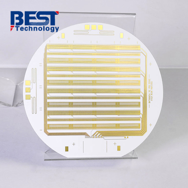
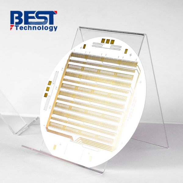
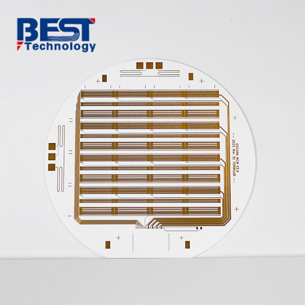
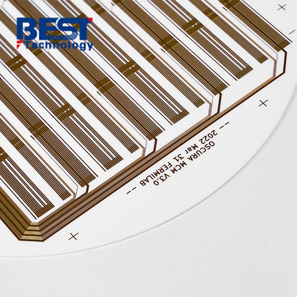
DPC Ceramic PCB Custom For New Energy Vehicles


Board thickness: 0.635mm+/- 0.1mm
Conductor: 35um copper
Solder mask: White
Silkscreen: N/A
Surface finishing: ENIG 1u’’
Application: Lithium battery
| Item1 | DPC Capabilities | |||||
|---|---|---|---|---|---|---|
|
Layer Count |
1-2 Layers |
|||||
|
Max Board Dimension |
120mmx180mm | |||||
|
Min Board Thickness |
0.15mm |
|||||
|
Max Board Thickness |
6.0mm |
|||||
|
Conductor Thickness |
50/50μm |
|||||
|
Min Line Width/Line Space |
3/3mil (0.075/0.075mm) |
|||||
|
Substrate Type |
AI2O3, ALN, Si3N4 |
|||||
|
Substrate Thickness |
0.15-6mm |
|||||
|
Min Hole Diameter |
100μm |
|||||
|
Min Hole Spacing |
250μm |
|||||
|
Min PAD Ring(Single) |
0.125mm |
|||||
|
PTH Wall Thickness |
8um |
|||||
|
Min Solder PAD Dia |
0.25mm |
|||||
|
Min Soldermask Bridge |
Green Oil 130μm; Others 150μm |
|||||
|
Min BAG PAD Margin |
0.3mm |
|||||
|
PTH/NPTH Dia Tolerance |
0.05/0.075mm |
|||||
|
Hole Position Deviation |
50-75μm |
|||||
|
Outline Tolerance |
Laser: +/-0.13mm |
|||||
|
Line Width/Spac Tolerance |
±20% |
|||||
|
Surface Treatment |
OSP/Immersion Gold/Nickel Plated Gold/Immersion Silver/Nickel Plated |
|||||
|
Thermal Stress |
7.3pmm/k |
|||||
| Item2 | Attribute | ||
|---|---|---|---|
|
Brand |
CeramTec / GTT / Huaqing / Laird / Maruwa / Rogers / Toshiba |
||
|
Base Material |
AI2O3 |
||
|
Base Material Thickness (exclude conductor) |
0.15-6mm |
||
|
Thermal Conductivity |
24-170W/mk |
||
|
Soldermask Type |
Aluminum Oxide |
||
|
Tg Value |
800℃ |
||
|
Halogen Free |
No |
||
|
Breakdown Voltage |
15 KV/mm |
||
|
Dielectric Constant (MHZ) |
9.4 (1MHz); 9.1 (13GHz) |
||
|
Water Absorption |
≤0.5% |
||
|
ROHS |
Yes |
||
|
Flammability |
Grade A |
||
|
Thermal Conductivity (W/m.K, or W/m.C) |
24-170 W/mk |
||
|
Dielectric Strength |
>15 KV/mm |
||
|
Wrap & Twist |
3% |
||
| Prototype(<1m²) | Layers | Normal Service | Expedited Service |
|---|---|---|---|
|
DPC Ceramic PCB |
1 Layer |
DPC: 2 - 3 weeks |
DPC: 1.5 weeks |
|
2 Layers |
DPC: 2 - 3 weeks |
DPC: 1.5 weeks |
| Production | Layers | Normal Service | Expedited service |
|---|---|---|---|
|
DPC Ceramic PCB |
1 Layer |
DPC: 3 - 4 weeks |
DPC: 1.5 - 2 weeks |
|
2 Layers |
DPC: 3 - 4 weeks |
DPC: 1.5 - 2 weeks |
Why Ceramic PCB has such excellent performance?
Advanced Ceramic Materials: Ceramic PCBs are constructed using high-quality materials such as alumina (Al2O3), aluminum nitride (ALN), or beryllium oxide (BeO). These materials offer excellent thermal conductivity, electrical insulation, and mechanical strength.
Conductors: Depending on the technology used, ceramic PCBs employ different conductive materials. Thin and thick film technology typically utilizes silver palladium (AgPd) or gold-palladium (AuPd), while Direct Copper Bonded (DCB) PCBs exclusively use copper conductors. These conductive materials ensure reliable electrical connectivity and efficient signal transmission.
Wide Temperature Range: Ceramic PCBs can operate in extreme temperatures ranging from -55°C to 850°C. This makes them suitable for applications in environments with significant temperature variations.
High Thermal Conductivity: Ceramic PCBs exhibit impressive thermal conductivity values, ranging from 24W/m-K to 28W/m-K for alumina, 150W/m-K to 240W/m-K for aluminum nitride, and 220W/m-K to 250W/m-K for beryllium oxide. This high thermal conductivity enables efficient heat dissipation, preventing component overheating and ensuring optimal performance.
DPC Ceramic PCB Specification:
|
Substrate material: |
Al2O3 |
|
Board thickness: |
0.635mm+/-0.1mm |
|
Conductor: |
35um copper |
|
Solder mask: |
White |
|
Silkscreen: |
N/A |
|
Surface finishing: |
ENIG 1u’’ |
|
Application: |
Lithium battery |
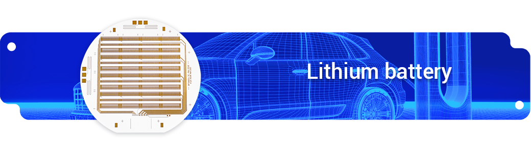
Background:
Lithium Technology is a leading manufacturer of lithium battery
Artificial intelligence and environmental protection are recommended to launch electric cars in the automotive industry, which mainly store electricity through batteries, using dpc ceramic substrates as lithium batteries to achieve better current and heat dissipation functions, and promote market demand for new energy vehicles.
PCB challenge:
The substrate thickness is too thin and it is not easy to set the laser energy, if too high the cutting-edge will become black easily.
Solution:
After checking the gerber file and understanding the end-application, our team suggested to use aluminum nitride material as the base since it has the good thermal management than aluminum oxide and optimized the line width to smooth the production.
To overcome the black edge challenge, we fabricated the first article for laser energy evaluation, and after several experiments, we got the best energy that can ensure the edge still keep the original color and protect the edge well.
Result and Benefits:
After receiving the ceramic PCB, customer tested all the boards first and all of them passed. Then they bonded the board into the converter and found the thermal conductivity was greatly improved than previous chip, meanwhile, the durability also better than normal circuit boards. “It is really a big innovation for us”, they said, they praised our professionalism and committed that we will be the first choice if they need ceramic PCB again.

 Products
 About us
 Contact us


