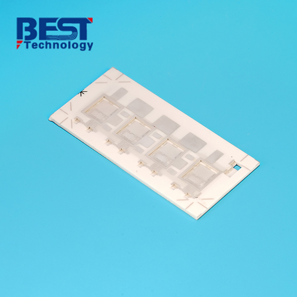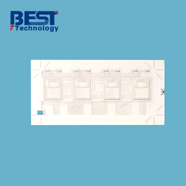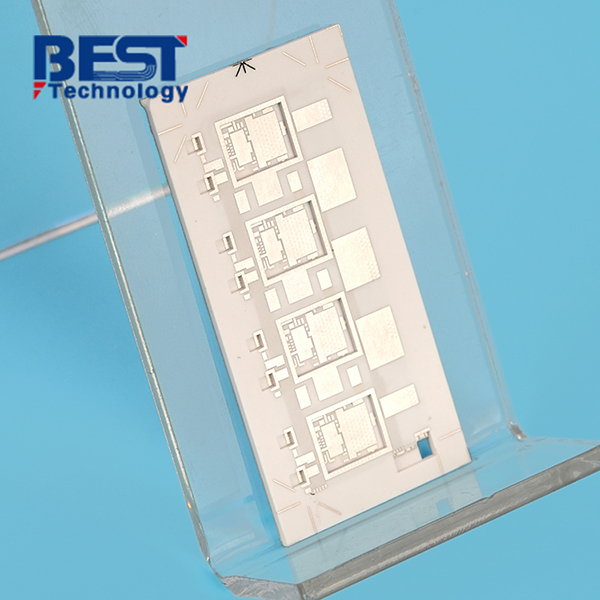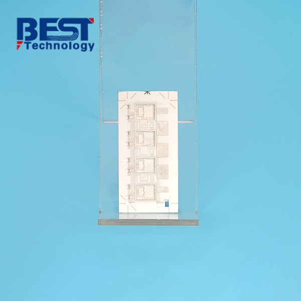
EPS Power Systems PCB Design LTCC Ceramic Substrate


Board Thickness: 1.0mm
Conductor: 0.1umTiW+3.0um Ni
Solder Mask: N/A
Silkscreen: N/A
Surface Finishing: N/A
Application: EPS Power Systems
| Item1 | LTCC Capabilities | |||||
|---|---|---|---|---|---|---|
|
Layer Count |
4-64 Layers |
|||||
|
Max Board Dimension |
150mm×150mm |
|||||
|
Min Board Thickness |
Single layer 0.1mm, total thickness 0.15mm |
|||||
|
Max Board Thickness |
Single layer 0.25mm, total thickness 6mm |
|||||
|
Conductor Thickness |
6-12μm (the surface layer can be thickened to 80μm) |
|||||
|
Min Line Width/Line Space |
150μm (surface layer can be refined to 50μm) |
|||||
|
Substrate Type |
Al2O3 |
|||||
|
Substrate Thickness |
0.15-6mm |
|||||
|
Min Hole Diameter |
100μm |
|||||
|
Min Hole Spacing |
250μm |
|||||
|
Min PAD Ring(Single) |
0.125mm |
|||||
|
PTH Wall Thickness |
N/A |
|||||
|
Min Solder PAD Dia |
0.1mm |
|||||
|
Min Soldermask Bridge |
75μm |
|||||
|
Min BAG PAD Margin |
0.635mm |
|||||
|
PTH/NPTH Dia Tolerance |
10μm |
|||||
|
Hole Position Deviation |
30-40μm |
|||||
|
Outline Tolerance |
Laser cutting: 0.005; Die stamping: 0.005 |
|||||
|
Line Width/Spac Tolerance |
±20% |
|||||
|
Surface Treatment |
Immersion Gold/Nickel Palladium Gold (Surface treatment is not recommended) |
|||||
|
Thermal Stress |
7.3ppm/K |
|||||
| Item2 | Attribute | ||
|---|---|---|---|
|
Base Material |
DP951,DP9K7, Ferro-A6-M |
||
|
Base Material Thickness (exclude conductor) |
0.15-6mm |
||
|
Thermal Conductivity |
17W/mk |
||
|
Soldermask Type |
Aluminum Oxide |
||
|
Tg Value |
800℃ |
||
|
Halogen Free |
No |
||
|
Breakdown Voltage |
9.4 (1MHz); 9.1 (13GHz) |
||
|
Dielectric Constant (MHZ) |
≤0.5% |
||
|
Water Absorption |
0% |
||
|
ROHS |
Yes |
||
|
Flammability |
Grade A |
||
|
Thermal Conductivity (W/m.K, or W/m.C) |
17W/mk |
||
|
Dielectric Strength |
15KV/mm |
||
|
Wrap & Twist |
0.003 |
||
| Prototype(<1m²) | Layers | Normal Service | Expedited Service |
|---|---|---|---|
|
LTCC Ceramic PCB |
6 Layers |
6 - 8 weeks |
3 - 4 weeks |
|
8 Layers |
6 - 8 weeks |
3 - 4 weeks |
|
|
10 Layers |
6 - 8 weeks |
3 - 4 weeks |
|
|
>10 Layers |
6 - 8 weeks |
3 - 4 weeks |
| Mass Production | Layers | Normal Service | Expedited service |
|---|---|---|---|
|
LTCC Ceramic PCB |
6 Layers |
7 - 9 weeks |
4 - 5 weeks |
|
8 Layers |
7 - 9 weeks |
4 - 5 weeks |
|
|
10 Layers |
7 - 9 weeks |
4 - 5 weeks |
|
|
>10 Layers |
7 - 9 weeks |
5 - 6 weeks |
Understanding LTCC Ceramic PCBs
LTCC Ceramic PCBs are a type of multilayer circuit board that utilizes Low-Temperature Co-fired Ceramic technology. These PCBs consist of multiple layers of ceramic material with embedded conductive traces and vias. The ceramic material used, such as alumina or aluminum nitride, offers excellent thermal properties.
LTCC Ceramic PCBs leverage the ceramic material's ability to dissipate heat efficiently while providing electrical insulation. This unique combination makes them ideal for applications where high-frequency signals, miniaturization, and heat dissipation are crucial.
Advantages of LTCC Ceramic PCBs
Low thermal resistance for effective heat dissipation: LTCC Ceramic PCBs exhibit low thermal resistance, allowing rapid heat transfer from the electronic components to the outer layers of the PCB. This enables efficient heat dissipation and prevents temperature-related performance degradation.
Excellent insulation properties for electrical safety: The ceramic material used in LTCC Ceramic PCBs provides excellent electrical insulation. This ensures reliable isolation between conductive traces, reducing the risk of short circuits and electrical malfunctions.
Suitable for miniaturized and high-frequency applications: LTCC Ceramic PCBs are well-suited for applications that require miniaturization and high-frequency signal transmission. They find extensive use in sectors such as telecommunications, aerospace, medical devices, and wireless communication systems.
LTCC Ceramic PCBs are highly advantageous in applications where effective heat dissipation, electrical insulation, and high-frequency performance are essential.
Background:
Customer Background:
AutoDrive Technologies is an automotive technology company specializing in EPS systems. They were seeking a reliable solution to enhance the performance and reliability of their EPS control modules.
Project Challenges:
AutoDrive Technologies faced challenges related to thermal management and signal integrity in their EPS power systems. They needed a solution that could efficiently dissipate heat, maintain high-speed signal transmission, and withstand harsh automotive environments.
Solution:
We collaborated closely with AutoDrive Technologies to develop custom LTCC ceramic PCBs for their EPS control modules. Our team of experts optimized the PCB layout, utilizing LTCC ceramic material for its excellent thermal conductivity and electrical properties. We offered customization options to accommodate AutoDrive Technologies' specific EPS system requirements. The LTCC ceramic PCBs were designed to integrate seamlessly with their existing control modules, simplifying the integration process and reducing overall system complexity. Benefits of LTCC ceramic PCB:
1. Thermal Management: LTCC ceramic PCBs offered excellent thermal conductivity, enabling efficient heat dissipation in EPS control modules. This resulted in improved performance, increased reliability, and extended lifespan of the systems.
2. Signal Integrity: LTCC ceramic material provided low dielectric losses and high signal transfer capabilities, ensuring reliable and high-speed signal transmission in EPS control modules. This contributed to enhanced system responsiveness and accuracy.
Result and benefit:
AutoDrive made a great success when apply the LTCC ceramic PCB into their EPS system, and by means of this innovation, they won some valued customers in the Canton fair. And obviously, we also became their reliable PCB supplier in Shenzhen.


 HOME
HOME


