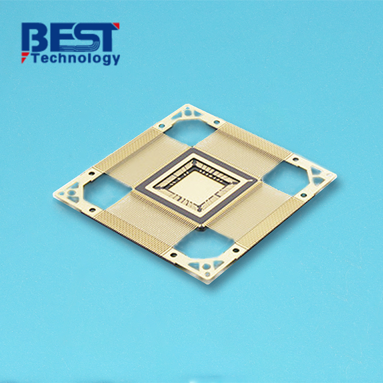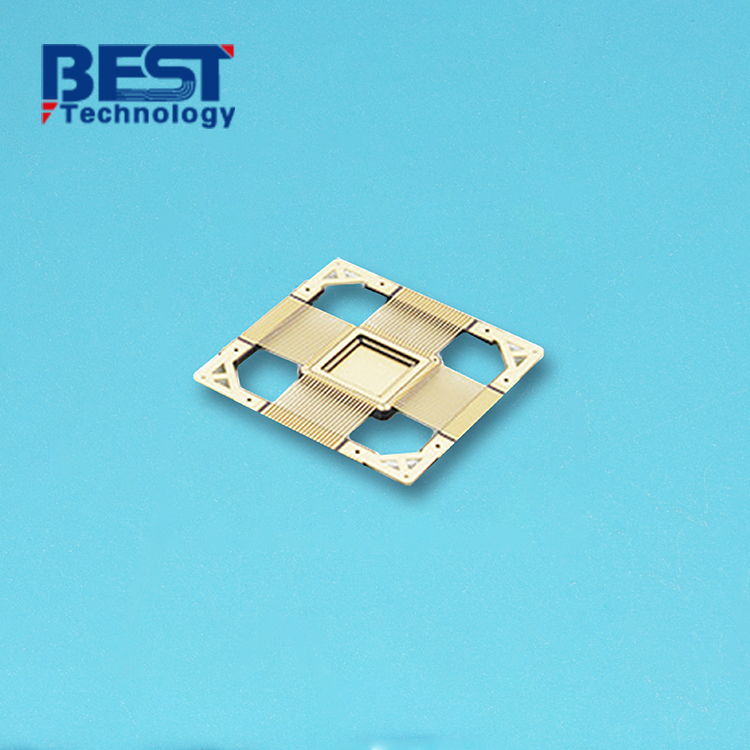
HTCC Ceramic Substrate PCB Design Making For Clock Amplifier


Working Temperature: -40-300℃
Conductor Thickness: 2um - 12um
LS/LW: 150um (Surface layer can be refined to 50μm)
Application: Clock Amplifier
| Item1 | HTCC Capabilities | |||||
|---|---|---|---|---|---|---|
|
Layer Count |
4-64 Layers |
|||||
|
Max Board Dimension |
150*150mm |
|||||
|
Min Board Thickness |
1Lay: 0.1mm 0.15mm |
|||||
|
Max Board Thickness |
1Lay: 0.25mm 6.0mm |
|||||
|
Conductor Thickness |
2um - 12um (Surface layer can be thickened to 80μm) |
|||||
|
Min Line Width/Line Space |
150um (Surface layer can be refined to 50μm) |
|||||
|
Substrate Type |
AI203 |
|||||
|
Substrate Thickness |
0.15-6um |
|||||
|
Min Hole Diameter |
100um |
|||||
|
Min Hole Spacing |
250um |
|||||
|
Min PAD Ring(Single) |
0.125mm |
|||||
|
PTH Wall Thickness |
No |
|||||
|
Min Solder PAD Dia |
0.1mm |
|||||
|
Min Soldermask Bridge |
75um |
|||||
|
Min BAG PAD Margin |
0.635mm |
|||||
|
PTH/NPTH Dia Tolerance |
10um |
|||||
|
Hole Position Deviation |
30-40um |
|||||
|
Outline Tolerance |
Laser: 0.005mm;Die Punch: 0.005mm |
|||||
|
Line Width/Spac Tolerance |
±20μm |
|||||
|
Surface Treatment |
Nickel-plated Gold |
|||||
|
Thermal Stress |
7.3ppm/K |
|||||
| Item2 | Attribute | ||
|---|---|---|---|
|
Brand |
CeramTec / GTT / Huaqing / Laird / Maruwa / Rogers / Toshiba |
||
|
Base Material |
AI203 |
||
|
Base Material Thickness (exclude conductor) |
0.15-6mm |
||
|
Thermal Conductivity |
17W/mk |
||
|
Soldermask Type |
AlN |
||
|
Tg Value |
800℃ |
||
|
Halogen Free |
No |
||
|
Breakdown Voltage |
15KV/mm |
||
|
Dielectric Constant (MHZ) |
9.4(1MHz) 9.1(13GHz) |
||
|
Water Absorption |
≤0.5% |
||
|
ROHS |
Yes |
||
|
Flammability |
A Level |
||
|
Thermal Conductivity (W/m.K, or W/m.C) |
17W/mk |
||
|
Dielectric Strength |
15KV/mm |
||
|
Wrap & Twist |
0.003 |
||
| Prototype(<1m²) | Layers | Normal Service | Expedited Service |
|---|---|---|---|
|
HTCC Ceramic PCB |
6 Layer |
6 - 8 weeks |
3 - 4 weeks |
|
8 Layers |
6 - 8 weeks |
3 - 4 weeks |
|
|
10 Layers |
6 - 8 weeks |
3 - 4 weeks |
|
|
Above 10 Layers |
6 - 8 weeks |
3 - 4 weeks |
| Production | Layers | Normal Service | Expedited service |
|---|---|---|---|
|
HTCC Ceramic PCB |
6 Layer |
7 - 9 weeks |
4 - 5 weeks |
|
8 Layers |
7 - 9 weeks |
4 - 5 weeks |
|
|
10 Layers |
7 - 9 weeks |
4 - 5 weeks |
|
|
Above 10 Layers |
7 - 9 weeks |
5 - 6 weeks |
How do we serve you?
Step one:
Our expertise lies in producing ceramic boards with superior flatness and precise printed resistor values, ensuring exceptional performance for your applications.
Step Two:
We offer flexible custom layout services, tailoring the ceramic boards to your specific design requirements. This ensures a perfect match between the board and your application.
Step Three:
Our knowledgeable technical support team is available to assist you throughout the design and production process. We are committed to resolving any issues promptly and ensuring a smooth experience.
Step Four:
We prioritize on-time delivery, ensuring your project stays on schedule. Additionally, we provide competitive pricing to meet your budgetary requirements.
Step Five:
Our manufacturing takes place in a state-of-the-art 2000 dust-free workshop, ensuring a clean and controlled environment for production.
All processes undergo rigorous quality control measures to ensure the highest standards of quality and reliability. By relying on our high-quality ceramic boards, custom layout services, professional technical support, on-time delivery, competitive pricing, and stringent quality control, we aim to exceed your expectations and provide you with the best possible experience.

Background:
Precision Timing Systems specializes in the development of high-precision clock amplifiers used in critical timing applications, such as telecommunications and data centers. They required PCBs that could support precise clock signal amplification, maintain signal integrity, and provide robust performance under demanding conditions.
Solution:
Precision Timing Systems selected HTCC ceramic PCBs for their clock amplifier modules. The HTCC ceramic PCBs offered low signal loss, high insulation resistance, and excellent thermal stability, ensuring accurate and reliable clock signal amplification. The robust mechanical strength of the ceramic material enabled the PCBs to withstand challenging environmental conditions and mechanical stresses.
Result and Benefits:
The adoption of HTCC ceramic PCBs in Precision Timing Systems' clock amplifier modules resulted in improved timing accuracy and reliability. The low signal loss and high insulation resistance provided by the PCBs contributed to precise clock signal amplification, ensuring accurate synchronization in critical timing applications. The robustness and thermal stability of HTCC ceramic PCBs ensured consistent performance even in demanding environments.


 HOME
HOME


