


 HOME
HOME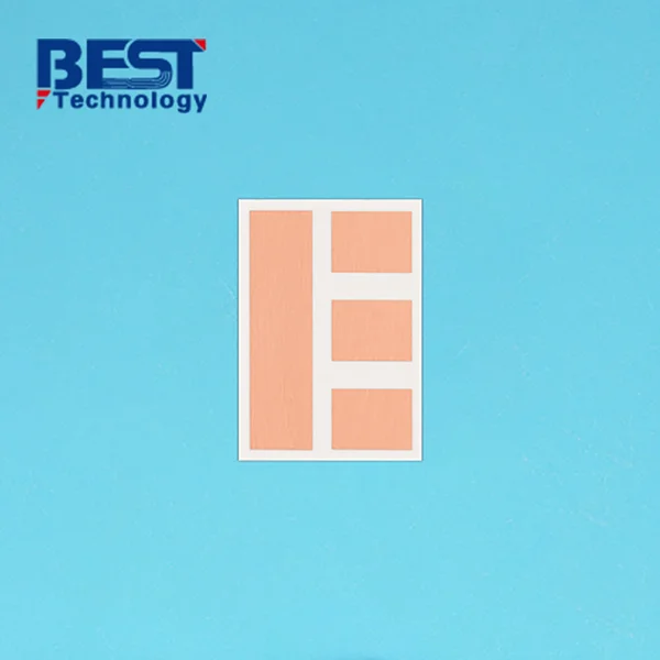
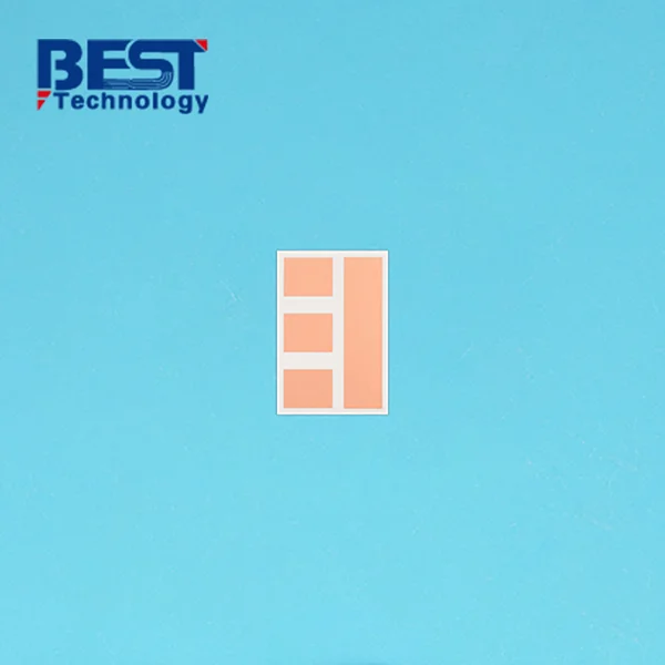
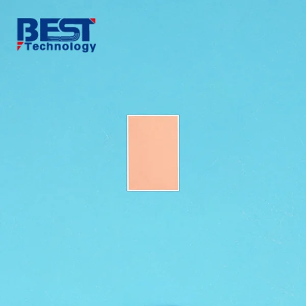
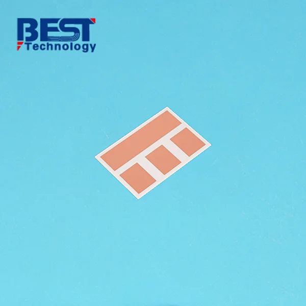
Thin film ceramic PCB Design Fabrication For Wireless Communication


Board Thickness: 1.0mm
Conductor: 0.1umTi+0.2mm Pt+3.0um Au
Solder Mask: N/A
Silkscreen: N/A
Surface Finishing: N/A
Application: Wireless Communication
| Item1 | Thin Film Capabilities | Special Needs |
| Circuit layers | 1~2 Layers | N/A |
| Product Unit Size | 0.5mmx0.5mm-200mmx200mm | 0.25mmx0.25mm |
| Substrate Thickness Tolerance | ≤ ± 10% | ±0.02mm |
| Element Size Tolerance | ±0.05mm | ±0.03mm |
| Minimum Line Width@Thickness<3μm | 20μm | 10μm |
| Line Width Accuracy | ±5μm | ±2μm |
| Forecast Minimum Size Of Gold-tin Solder | 100μm*100μm | 50μm*50μm |
| Distance From Wire To Substrate Edge | 50μm | min 20μm |
| Minimum Land Size Around Vias | ≥Aperture+50μm | N/A |
| Front, Back, Multilayer Alignment Accuracy | ≤ ± 5μm | ± 1μm |
| Front, Side Alignment Accuracy | ≤ 20μm | N/A |
| Available Cutter Width | 0.1, 0.15, 0.2mm | N/A |
| Cutting Accuracy Of Grinding Wheel | ± 50μm | ± 20μm |
| Laser Cutting Precision | ± 20μm | N/A |
| Minimum Hole Diameter | 0.5*Board Thickness | N/A |
| Aperture Tolerance | ± 10% | N/A |
| Solid Hole Diameter | 0.075, 0.1mm | N/A |
| Item2 | Attributes | Special Needs |
| Brand | BSTCeramicPCB | N/A |
| Substrate type | AlN, Al2O3, Si, Quartz, Glass-ceramic, Diamond, Sapphire | N/A |
| Substrate Roughness (Ra) | ≤0.1μm | ≤0.05μm |
| Coating Type | Metal film, resistive film, dielectric film, functional film, etc. | N/A |
| Film Thickness Tolerance | ±20% | ±5% |
| Resistive film square resistance | 10-200 | N/A |
| Resistance value accuracy (laser trimmable) | ±0.1% | ±0.05% |
| Resistance value accuracy (no laser trimming) | ±5% | ±3% |
| Temperature coefficient of resistance | ±25ppm | min±10ppm |
| Rapid Prototype | Layer | Normal Delivery | Expedited Service |
| Thin Film Ceramic PCB | 1 | 3-4.5 Weeks | 2-2.5 Weeks |
| 2 | 4-6 Weeks | 2-2.5 Weeks |
| Mass Production | Layer | Normal Delivery | Expedited Service |
| Thin Film Ceramic PCB | 1 | 4-5 Weeks | 2-3 Weeks |
| 2 | 4-6 Weeks | 2-3 Weeks |
A key differentiator is their smaller size when comparing thin-film circuits to thick-film ceramic PCBs. Thin-film circuits are ideal for applications requiring high accuracy, great stability, and excellent performance, especially in analog circuits. They are particularly well-suited for microwave circuits. However, it's essential to note that the manufacturing equipment for thin-film circuits is more expensive, leading to higher production costs compared to thick-film ceramic PCBs. Despite this, the benefits of thin-film ceramic PCBs, such as their superior performance and suitability for specialized circuits, make them a preferred choice for specific applications.
Why Best Technology?
- Rich Experience: With over 17 years of experience in the ceramic board industry, we possess in-depth knowledge and can cater to a wide range of customer requirements.
- In-House Production: Best Technology boasts its own ceramic board factory and SMT production workshop, enabling us to have direct control over the manufacturing process, ensuring top-notch product quality and on-time deliveries.
- Technical Expertise: Our team is highly skilled and experienced, offering customized solutions that meet the highest standards of thermal stability, chemical resistance, and electrical performance, tailored to our clients' needs.
- Diverse Applications: Best Technology's ceramic boards find applications across various industries, including communication, electronics, medical, aerospace, and more. Whatever your industry demands, we have the most suitable solutions for you.
- Quality Assurance and Customer Support: We are committed to delivering excellent products and services to our customers. Our stringent quality control measures guarantee the finest products, and our prompt technical support ensures customer satisfaction.
At Best Technology, you can expect ceramic board products of unparalleled experience, cutting-edge technology, and customized solutions. We look forward to establishing a partnership with you to drive your projects to success. For any inquiries or further information, please feel free to contact us.
Customer Background:
A leading telecommunications company specializing in wireless communication systems and devices for global networks.
Customer Project Requirements:
They required a high-performance and reliable circuit board for their latest 5G wireless communication module, designed to handle ultra-fast data transfer rates and support advanced communication protocols. The board needed to support high-frequency operation to ensure seamless and low-latency data transmission.
Project Challenges:
To meet the demanding requirements of 5G communication, the Thin Film Ceramic PCB had to achieve ultra-thin conductive layers, typically below 1 micron (10-13μm), and tight tolerances to minimize signal losses and interference. The challenge was to maintain precise circuitry while handling high frequencies, ensuring signal integrity and low transmission losses.
Achievements:
After successfully producing the sample boards, the customer extensively tested them and was highly impressed with the performance and signal integrity achieved by the Thin Film Ceramic PCBs. The boards successfully met their stringent requirements for high-frequency communication. As a result of this successful collaboration, the customer placed a significant bulk order for the Thin Film Ceramic PCBs to integrate into their 5G wireless communication modules. The high customer satisfaction and repeat orders further solidified our position as a reliable partner in the telecommunications industry.

 Products
 About us
 Contact us


