


 HOME
HOME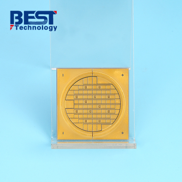
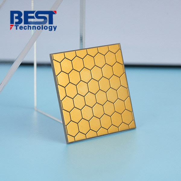
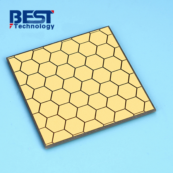
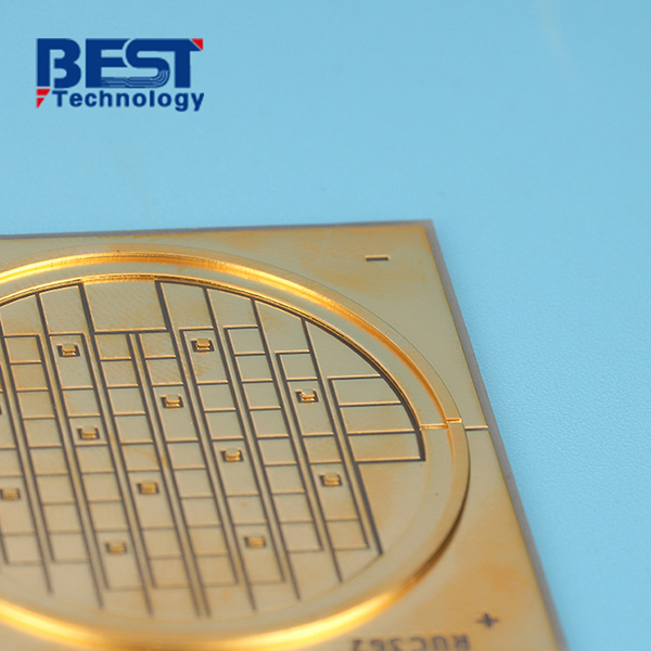
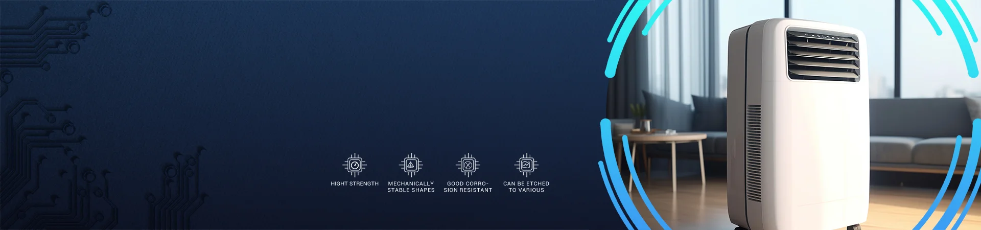
DBC/DCB Ceramic Substrate PCB For Portable Cooling Device


Board Thickness: 1.5mm+/-10%
Conductor: 100um copper
Solder Mask: N/A
Silkscreen: N/A
Surface Finishing: ENEPIG 3u’’
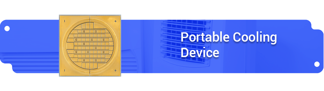
Application: Portable Cooling Device
| Item1 | DCB/DBC Capabilities | |||||
|---|---|---|---|---|---|---|
|
Layer Count |
1-2 Layers |
|||||
|
Max Board Dimension |
120mmx180mm |
|||||
|
Min Board Thickness |
0.254mm |
|||||
|
Max Board Thickness |
2.0mm |
|||||
|
Conductor Thickness |
100-600μm |
|||||
|
Min Line Width/Line Space |
300/300μm |
|||||
|
Substrate Type |
AI2O3 |
|||||
|
Substrate Thickness |
0.254-2.0mm |
|||||
|
Min Hole Diameter |
0.25mm (No Via Hole) |
|||||
|
Min Hole Spacing |
250μm |
|||||
|
Min PAD Ring(Single) |
0.125mm |
|||||
|
PTH Wall Thickness |
N/A |
|||||
|
Min Solder PAD Dia |
0.5mm |
|||||
|
Min Soldermask Bridge |
Green Oil 130μm; Others 150μm |
|||||
|
Min BAG PAD Margin |
0.35mm |
|||||
|
PTH/NPTH Dia Tolerance |
0.075mm |
|||||
|
Hole Position Deviation |
75μm |
|||||
|
Outline Tolerance |
Laser: +/-0.13mm |
|||||
|
Line Width/Spac Tolerance |
±20% |
|||||
|
Surface Treatment |
OSP/Immersion Gold/Nickel Plated Gold/Immersion Silver/Nickel Plated |
|||||
|
Thermal Stress |
7.3ppm/k |
|||||
| Item2 | Attribute | ||
|---|---|---|---|
|
Brand |
CeramTec / GTT / Huaqing / Laird / Maruwa / Rogers / Toshiba |
||
|
Base Material |
AI2O3 |
||
|
Base Material Thickness (exclude conductor) |
0.45-3.2mm |
||
|
Thermal Conductivity |
24-170W/mk |
||
|
Soldermask Type |
Aluminum Oxide |
||
|
Tg Value |
800℃ |
||
|
Halogen Free |
No |
||
|
Breakdown Voltage |
>15KV/mm |
||
|
Dielectric Constant (MHZ) |
9.4 (1MHz); 9.1 (13GHz) |
||
|
Water Absorption |
≤0.5% |
||
|
ROHS |
Yes |
||
|
Flammability |
Grade A |
||
|
Thermal Conductivity (W/m.K, or W/m.C) |
24-170W/mk |
||
|
Dielectric Strength |
15KV/mm |
||
|
Wrap & Twist |
3% |
||
| Prototype(<1m²) | Layers | Normal Service | Expedited Service |
|---|---|---|---|
|
DCB/DBC Ceramic PCB |
1 Layer |
2 - 3 weeks |
1.5 weeks |
|
2 Layers |
2 - 3 weeks |
1.5 weeks |
| Production | Layers | Normal Service | Expedited service |
|---|---|---|---|
|
DCB/DBC Ceramic PCB |
1 Layer |
3 - 4 weeks |
1.5 - 2 weeks |
|
2 Layers |
3 - 4 weeks |
1.5 - 2 weeks |
With the expanding use of VLSI and the growth of SMT, the design of organic laminated PCBs faces considerable difficulties in terms of heat dissipation. This challenge arises from the low thermal conductivity of most conventional PCB materials. However, ceramics offer a compelling solution due to their exceptional thermal properties.
Compared to ordinary PCBs, ceramics exhibit a thermal conductivity that is approximately 90 times higher than that of epoxy glass fiber, which is commonly used in traditional PCBs. This high thermal conductivity enables ceramic PCBs to efficiently dissipate heat, making them highly suitable for applications where effective thermal management is essential. By facilitating excellent conduction cooling, ceramic PCBs prevent excessive heat buildup that can adversely affect the performance and reliability of electronic components.
DBC Ceramic PCB Specification:
|
Substrate material: |
AlN |
|
Board thickness: |
0.56mm+/-0.1mm |
|
Conductor: |
100um copper |
|
Solder mask: |
N/A |
|
Silkscreen: |
N/A |
|
Surface finishing: |
ENEPIG 3u’’ |
|
Application: |
Portable cooling device |
Bioly Electronics is a company that specializes in developing innovative technologies for the life sciences industry. They are planning to design a new electrochemical biosensor for a research project, and they have decided to use a ceramic PCB as the base plate for the biosensor.
At the initial step in the design process was to select the appropriate substrate material for the biosensor. After considering various options, Bioly Electronics chose a double-sided DBC ceramic PCB due to its excellent electrical insulation and high thermal conductivity. The ceramic substrate provides a stable and reliable platform for the biosensor to function on.
Project Challenge:
1.The copper thickness required 300um, it is not easy to plate such thick copper in one time.
2.The copper surface should have good flatness, it is difficult to control especially copper needs to be plated multiple times to achieve 300um.
3. It is a big challengeA to protect the copper surface from scratch during the complex manufacturing process.

 Products
 About us
 Contact us


