


 HOME
HOME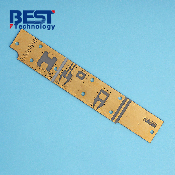
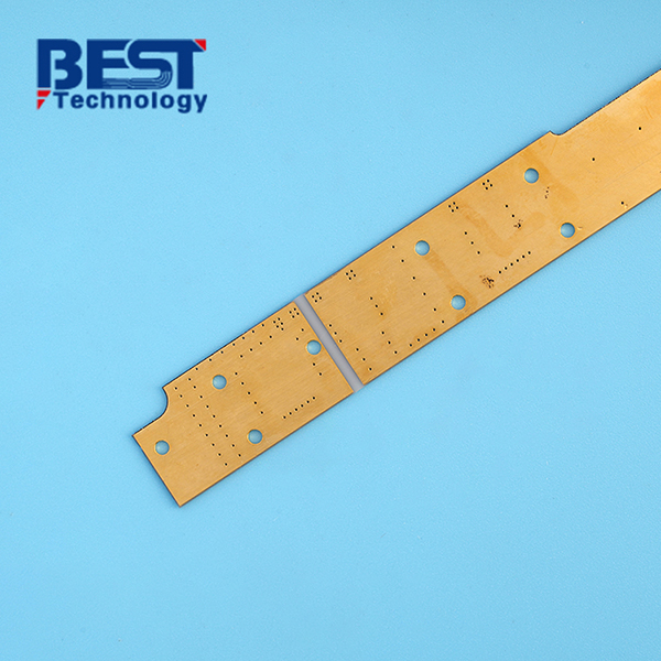
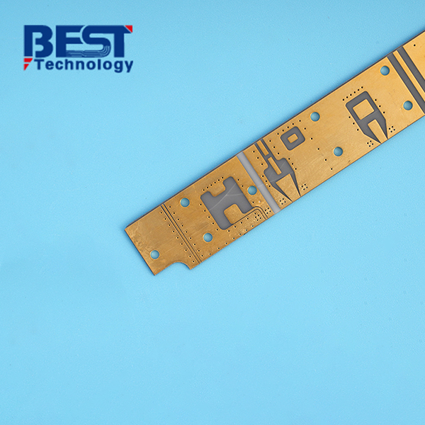
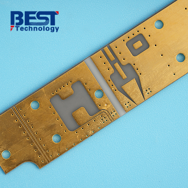
DCB Ceramic Substrate PCB For IGBT Semi-conductor


Board Thickness: 1.6mm+/-0.1mm
Conductor: 300um copper
Solder Mask: N/A
Silkscreen: N/A
Surface Finishing: ENEG 1u’’
Application: IGBT semi-conductor
| Item1 | DCB/DBC Capabilities | |||||
|---|---|---|---|---|---|---|
|
Layer Count |
1-2 Layers |
|||||
|
Max Board Dimension |
120mmx180mm |
|||||
|
Min Board Thickness |
0.254mm |
|||||
|
Max Board Thickness |
2.0mm |
|||||
|
Conductor Thickness |
100-600μm |
|||||
|
Min Line Width/Line Space |
300/300μm |
|||||
|
Substrate Type |
AI2O3 |
|||||
|
Substrate Thickness |
0.254-2.0mm |
|||||
|
Min Hole Diameter |
0.25mm (No Via Hole) |
|||||
|
Min Hole Spacing |
250μm |
|||||
|
Min PAD Ring(Single) |
0.125mm |
|||||
|
PTH Wall Thickness |
N/A |
|||||
|
Min Solder PAD Dia |
0.5mm |
|||||
|
Min Soldermask Bridge |
Green Oil 130μm; Others 150μm |
|||||
|
Min BAG PAD Margin |
0.35mm |
|||||
|
PTH/NPTH Dia Tolerance |
0.075mm |
|||||
|
Hole Position Deviation |
75μm |
|||||
|
Outline Tolerance |
Laser: +/-0.13mm |
|||||
|
Line Width/Spac Tolerance |
±20% |
|||||
|
Surface Treatment |
OSP/Immersion Gold/Nickel Plated Gold/Immersion Silver/Nickel Plated |
|||||
|
Thermal Stress |
7.3ppm/k |
|||||
| Item2 | Attribute | ||
|---|---|---|---|
|
Brand |
CeramTec / GTT / Huaqing / Laird / Maruwa / Rogers / Toshiba |
||
|
Base Material |
AI2O3 |
||
|
Base Material Thickness (exclude conductor) |
0.45-3.2mm |
||
|
Thermal Conductivity |
24-170W/mk |
||
|
Soldermask Type |
Aluminum Oxide |
||
|
Tg Value |
800℃ |
||
|
Halogen Free |
No |
||
|
Breakdown Voltage |
>15KV/mm |
||
|
Dielectric Constant (MHZ) |
9.4 (1MHz); 9.1 (13GHz) |
||
|
Water Absorption |
≤0.5% |
||
|
ROHS |
Yes |
||
|
Flammability |
Grade A |
||
|
Thermal Conductivity (W/m.K, or W/m.C) |
24-170W/mk |
||
|
Dielectric Strength |
15KV/mm |
||
|
Wrap & Twist |
3% |
||
| Prototype(<1m²) | Layers | Normal Service | Expedited Service |
|---|---|---|---|
|
DCB/DBC Ceramic PCB |
1 Layer |
2 - 3 weeks |
1.5 weeks |
|
2 Layers |
2 - 3 weeks |
1.5 weeks |
| Production | Layers | Normal Service | Expedited service |
|---|---|---|---|
|
DCB/DBC Ceramic PCB |
1 Layer |
3 - 4 weeks |
1.5 - 2 weeks |
|
2 Layers |
3 - 4 weeks |
1.5 - 2 weeks |
How can we assist you?
- Our expertise lies in manufacturing ceramic boards with exceptional flatness and precise printed resistor values.
- We provide flexible custom layout services, ensuring that your ceramic boards are tailored to your exact design requirements.
- Our dedicated technical support team is available to assist you at every step of the design and production process, promptly addressing any concerns or challenges.
- We prioritize timely delivery and offer competitive pricing options to our valued customers.
- All our manufacturing processes take place in a state-of-the-art 2000-class dust-free workshop, and we maintain stringent quality control measures throughout every stage of production.
DBC ceramic PCB specification:
|
Substrate material: |
AlN |
|
Board thickness: |
1.6mm+/-0.1mm |
|
Conductor: |
300um copper |
|
Solder mask: |
N/A |
|
Silkscreen: |
N/A |
|
Surface finishing: |
ENEG 1u’’ |
|
Application: |
IGBT semi-conductor |
Background:
Certa Electronics is a prominent manufacturer in the power electronics industry, specializing in the development and production of advanced semiconductor devices. With a focus on sustainable energy solutions, they cater to various sectors such as renewable energy, industrial automation, and electric mobility. Their commitment to innovation and quality has positioned them as a trusted partner in the market.
In one of their recent projects, our client successfully utilized DBC ceramic circuit boards in the design of Insulated Gate Bipolar Transistors (IGBTs). This application showcased the effectiveness and advantages of integrating ceramic circuit boards into IGBT semiconductors.
Project Challenge:
- Our client aimed to develop IGBT modules with enhanced performance and reliability for electric vehicle (EV) applications. The main challenge was to efficiently manage heat dissipation and ensure electrical insulation in the compact space of the module.
- The copper surface is easy to be oxidation during the manufacturing.
- Quality control is very strict since it is an EV part.
Solution:
To address the challenge, our client finally chose DBC ceramic circuit boards in their IGBT semiconductor design. The ALN (Aluminum Nitride) material was chosen for its exceptional thermal conductivity, electrical insulation properties, and mechanical stability.
Benefits And Outcomes:
The integration of DBC ceramic circuit boards in the IGBT semiconductor modules delivered several benefits:
1.Enhanced Thermal Management: The ALN-based DBC ceramic circuit boards provided efficient heat dissipation, maintaining optimal operating temperatures within the IGBT module. This resulted in improved performance, reduced thermal stress, and enhanced reliability.
2. Reliable Electrical Insulation: The ceramic circuit boards offered reliable electrical insulation, preventing short circuits and ensuring safe operation even in high-voltage applications. This enhanced the overall durability and safety of the IGBT semiconductors.
3.Space Optimization: The compact design of the ceramic circuit boards allowed for efficient space utilization within the IGBT modules. This enabled the client to develop smaller, lightweight, and more efficient EV power systems.

 Products
 About us
 Contact us


