


 HOME
HOME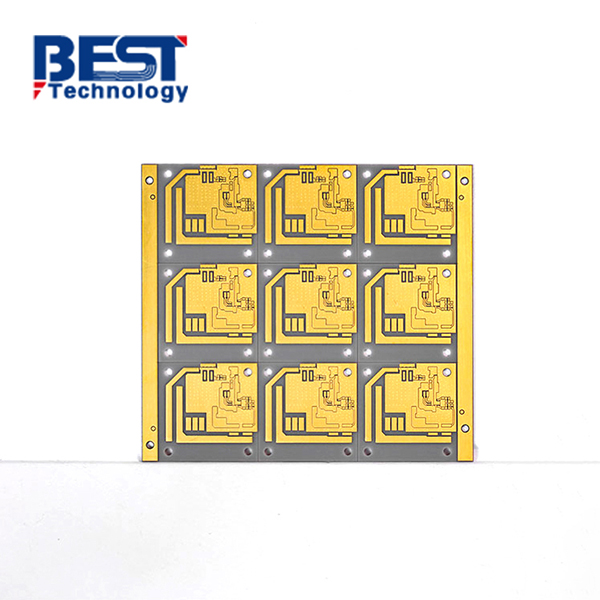
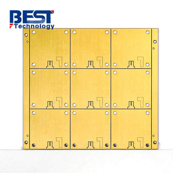
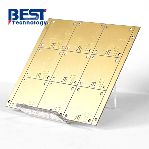
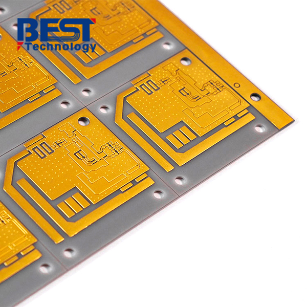
Double-sided Aluminum Nitride Filter Product DPC Ceramic Circuit Board For Stabilizer


Board thickness: 1.0mm+/-0.1mm
Conductor: 35um copper on both sides
Solder mask: N/A
Silkscreen: N/A
Surface finishing: ENEPIG 3u’’
Application: Stabilizer
| Item1 | DPC Capabilities | |||||
|---|---|---|---|---|---|---|
|
Layer Count |
1-2 Layers |
|||||
|
Max Board Dimension |
120mmx180mm | |||||
|
Min Board Thickness |
0.15mm |
|||||
|
Max Board Thickness |
6.0mm |
|||||
|
Conductor Thickness |
50/50μm |
|||||
|
Min Line Width/Line Space |
3/3mil (0.075/0.075mm) |
|||||
|
Substrate Type |
AI2O3, ALN, Si3N4 |
|||||
|
Substrate Thickness |
0.15-6mm |
|||||
|
Min Hole Diameter |
100μm |
|||||
|
Min Hole Spacing |
250μm |
|||||
|
Min PAD Ring(Single) |
0.125mm |
|||||
|
PTH Wall Thickness |
8um |
|||||
|
Min Solder PAD Dia |
0.25mm |
|||||
|
Min Soldermask Bridge |
Green Oil 130μm; Others 150μm |
|||||
|
Min BAG PAD Margin |
0.3mm |
|||||
|
PTH/NPTH Dia Tolerance |
0.05/0.075mm |
|||||
|
Hole Position Deviation |
50-75μm |
|||||
|
Outline Tolerance |
Laser: +/-0.13mm |
|||||
|
Line Width/Spac Tolerance |
±20% |
|||||
|
Surface Treatment |
OSP/Immersion Gold/Nickel Plated Gold/Immersion Silver/Nickel Plated |
|||||
|
Thermal Stress |
7.3pmm/k |
|||||
| Item2 | Attribute | ||
|---|---|---|---|
|
Brand |
CeramTec / GTT / Huaqing / Laird / Maruwa / Rogers / Toshiba |
||
|
Base Material |
AI2O3 |
||
|
Base Material Thickness (exclude conductor) |
0.15-6mm |
||
|
Thermal Conductivity |
24-170W/mk |
||
|
Soldermask Type |
Aluminum Oxide |
||
|
Tg Value |
800℃ |
||
|
Halogen Free |
No |
||
|
Breakdown Voltage |
15 KV/mm |
||
|
Dielectric Constant (MHZ) |
9.4 (1MHz); 9.1 (13GHz) |
||
|
Water Absorption |
≤0.5% |
||
|
ROHS |
Yes |
||
|
Flammability |
Grade A |
||
|
Thermal Conductivity (W/m.K, or W/m.C) |
24-170 W/mk |
||
|
Dielectric Strength |
>15 KV/mm |
||
|
Wrap & Twist |
3% |
||
| Prototype(<1m²) | Layers | Normal Service | Expedited Service |
|---|---|---|---|
|
DPC Ceramic PCB |
1 Layer |
DPC: 2 - 3 weeks |
DPC: 1.5 weeks |
|
2 Layers |
DPC: 2 - 3 weeks |
DPC: 1.5 weeks |
| Production | Layers | Normal Service | Expedited service |
|---|---|---|---|
|
DPC Ceramic PCB |
1 Layer |
DPC: 3 - 4 weeks |
DPC: 1.5 - 2 weeks |
|
2 Layers |
DPC: 3 - 4 weeks |
DPC: 1.5 - 2 weeks |
DPC technology refers to a special process that directly combines copper foil with alumina or aluminum nitride (one or both sides) at a suitable high temperature.
Basic parameter of DPC ceramic PCB
- Substrate thickness: 0.25mm, 0.38mm,0.50mm, 0.635mm, 0.8mm, 1.0mm, 1.5mm, 2.0mm, etc.
- Conductor: copper, the thickness can be 1/2OZ-10OZ
- Min line width and space: 0.12mm (mass production), 0.10mm (prototype)
- Finished product trace tolerance is +/-10%
- DPC ceramic PCB is suitable for wire-bonding products
- Solder mask is available
DPC Ceramic PCB specification:
|
Substrate material: |
Aluminum Nitride |
|
Board thickness: |
1.0mm+/-0.1mm |
|
Conductor: |
35um copper on both sides |
|
Solder mask: |
N/A |
|
Silkscreen: |
N/A |
|
Surface finishing: |
ENEPIG 3u’’ |
|
Application: |
Stabilizer |
Background:
FSS is a renowned electronics manufacturing company specializing in the production of high-quality voltage regulators. With a strong reputation for delivering reliable power management solutions, they serve diverse industries and have a keen focus on technological advancements. As a leading player in the market, our client is always seeking innovative approaches to enhance the performance and reliability of their products. The client approached us with a specific challenge related to their voltage regulator design. They were facing difficulties in achieving efficient thermal management, maintaining high electrical performance, and ensuring long-term reliability in their existing designs. These challenges were limiting their ability to meet the evolving demands of their customers and compete effectively in the market.
Project challenge:
The smallest holes in ceramic PCB must be plated with copper foil and have a 0.05mm tolerance, it is not easy to control during manufacturing.
Solution:
To address the client's challenges, we proposed the incorporation of DPC (Direct Printed Ceramic) circuit boards into their voltage regulator designs. We outlined the unique advantages of DPC technology and how it could significantly enhance their product performance. Upon implementing our proposed solution, the client experienced remarkable improvements in their voltage regulator designs. The DPC ceramic circuit boards successfully addressed the thermal management challenges, resulting in enhanced reliability and extended product lifespan. The superior electrical performance of DPC boards led to improved signal integrity and reduced EMI, meeting the stringent requirements of their customers.
Result and Benefits:
FSS team expressed great satisfaction with the outcome of the project. Our innovative solution not only resolved their existing challenges but also provided a competitive edge in the market. The client praised our expertise, responsiveness, and ability to deliver a tailored solution that met their specific needs. As a result, the client has continued to collaborate with us on subsequent projects and recommended our services to other industry players.

 Products
 About us
 Contact us


