


 HOME
HOME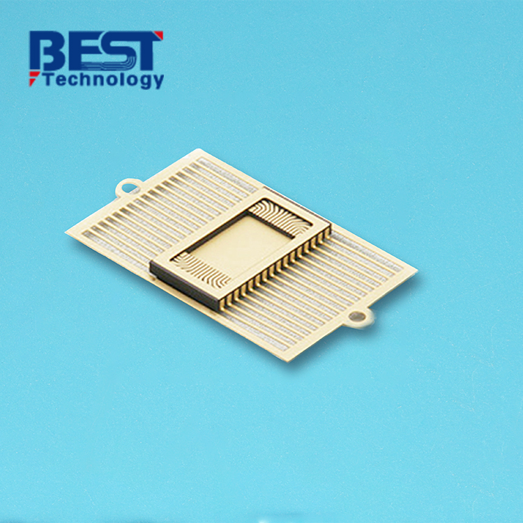
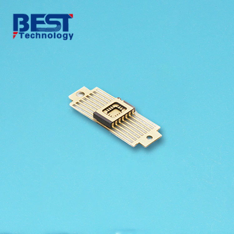
HTCC Substrate PCB Fabricate For Signal Converter


Working Temperature: -40-300℃
Conductor Thickness: 2um - 12um
LS/LW: 150um (Surface layer can be refined to 50μm)
Application: Signal Converter System
| Item1 | HTCC Capabilities | |||||
|---|---|---|---|---|---|---|
|
Layer Count |
4-64 Layers |
|||||
|
Max Board Dimension |
150*150mm |
|||||
|
Min Board Thickness |
1Lay: 0.1mm 0.15mm |
|||||
|
Max Board Thickness |
1Lay: 0.25mm 6.0mm |
|||||
|
Conductor Thickness |
2um - 12um (Surface layer can be thickened to 80μm) |
|||||
|
Min Line Width/Line Space |
150um (Surface layer can be refined to 50μm) |
|||||
|
Substrate Type |
AI203 |
|||||
|
Substrate Thickness |
0.15-6um |
|||||
|
Min Hole Diameter |
100um |
|||||
|
Min Hole Spacing |
250um |
|||||
|
Min PAD Ring(Single) |
0.125mm |
|||||
|
PTH Wall Thickness |
No |
|||||
|
Min Solder PAD Dia |
0.1mm |
|||||
|
Min Soldermask Bridge |
75um |
|||||
|
Min BAG PAD Margin |
0.635mm |
|||||
|
PTH/NPTH Dia Tolerance |
10um |
|||||
|
Hole Position Deviation |
30-40um |
|||||
|
Outline Tolerance |
Laser: 0.005mm;Die Punch: 0.005mm |
|||||
|
Line Width/Spac Tolerance |
±20μm |
|||||
|
Surface Treatment |
Nickel-plated Gold |
|||||
|
Thermal Stress |
7.3ppm/K |
|||||
| Item2 | Attribute | ||
|---|---|---|---|
|
Brand |
CeramTec / GTT / Huaqing / Laird / Maruwa / Rogers / Toshiba |
||
|
Base Material |
AI203 |
||
|
Base Material Thickness (exclude conductor) |
0.15-6mm |
||
|
Thermal Conductivity |
17W/mk |
||
|
Soldermask Type |
AlN |
||
|
Tg Value |
800℃ |
||
|
Halogen Free |
No |
||
|
Breakdown Voltage |
15KV/mm |
||
|
Dielectric Constant (MHZ) |
9.4(1MHz) 9.1(13GHz) |
||
|
Water Absorption |
≤0.5% |
||
|
ROHS |
Yes |
||
|
Flammability |
A Level |
||
|
Thermal Conductivity (W/m.K, or W/m.C) |
17W/mk |
||
|
Dielectric Strength |
15KV/mm |
||
|
Wrap & Twist |
0.003 |
||
| Prototype(<1m²) | Layers | Normal Service | Expedited Service |
|---|---|---|---|
|
HTCC Ceramic PCB |
6 Layer |
6 - 8 weeks |
3 - 4 weeks |
|
8 Layers |
6 - 8 weeks |
3 - 4 weeks |
|
|
10 Layers |
6 - 8 weeks |
3 - 4 weeks |
|
|
Above 10 Layers |
6 - 8 weeks |
3 - 4 weeks |
| Production | Layers | Normal Service | Expedited service |
|---|---|---|---|
|
HTCC Ceramic PCB |
6 Layer |
7 - 9 weeks |
4 - 5 weeks |
|
8 Layers |
7 - 9 weeks |
4 - 5 weeks |
|
|
10 Layers |
7 - 9 weeks |
4 - 5 weeks |
|
|
Above 10 Layers |
7 - 9 weeks |
5 - 6 weeks |
Best Technology provides a comprehensive range of ceramic packages that are renowned for their exceptional reliability. Our offerings include both custom-designed packages tailored to specific applications and standardized packages that are ideal for device evaluations. By utilizing our standard products during the evaluation stage, our customers can significantly reduce their initial investment costs. For further details regarding package forms and dimensions, please refer to the list of standard products outlined below.
Application:
Our ceramic packages cater to a wide range of industries, including industrial equipment and communications equipment. They are particularly well-suited for accommodating MPU (Microprocessing Units), ASIC (Application-Specific Integrated Circuits), and high-frequency devices.
Device Evaluations:
We understand the importance of thorough device evaluations prior to production. Therefore, our standardized packages are specifically designed to facilitate these evaluation processes efficiently. By utilizing our standard products, customers can save both time and resources while ensuring reliable performance.
Please reach out to us for optimized content tailored to your specific requirements or if you have any further queries. We are committed to providing the most suitable ceramic packages for your applications.

Background:
XYZ Communications required a PCB solution for their signal repeater devices, which amplify and relay wireless signals in telecommunications networks. The PCBs needed to support high-speed signal transmission, resist EMI, and maintain signal integrity in challenging environments.
Solution:
HTCC ceramic PCBs were chosen by XYZ Communications for their signal repeater devices. The ceramic material's high-frequency capabilities enabled efficient signal transmission, while the low dielectric loss ensured minimal signal degradation. The HTCC ceramic PCBs also provided excellent resistance to EMI, maintaining signal integrity in challenging environments.
Result and Benefits:
The HTCC ceramic PCBs proved to be a reliable choice for XYZ Communications' signal repeater devices. They enabled high-speed signal transmission with minimal losses, ensuring efficient signal amplification and relay. The resistance to EMI contributed to improved signal quality and reliability in telecommunications networks.

 Products
 About us
 Contact us


