


 HOME
HOME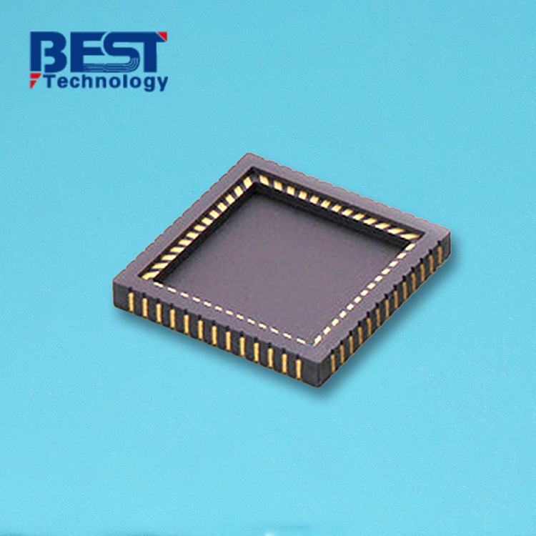
HTCC Ceramic Substrate Design Production For Defense Application


Working Temperature: -40-300℃
Conductor Thickness: 2um - 12um
LS/LW: 150um (Surface layer can be refined to 50μm)
Application: Defense System
| Item1 | HTCC Capabilities | |||||
|---|---|---|---|---|---|---|
|
Layer Count |
4-64 Layers |
|||||
|
Max Board Dimension |
150*150mm |
|||||
|
Min Board Thickness |
1Lay: 0.1mm 0.15mm |
|||||
|
Max Board Thickness |
1Lay: 0.25mm 6.0mm |
|||||
|
Conductor Thickness |
2um - 12um (Surface layer can be thickened to 80μm) |
|||||
|
Min Line Width/Line Space |
150um (Surface layer can be refined to 50μm) |
|||||
|
Substrate Type |
AI203 |
|||||
|
Substrate Thickness |
0.15-6um |
|||||
|
Min Hole Diameter |
100um |
|||||
|
Min Hole Spacing |
250um |
|||||
|
Min PAD Ring(Single) |
0.125mm |
|||||
|
PTH Wall Thickness |
No |
|||||
|
Min Solder PAD Dia |
0.1mm |
|||||
|
Min Soldermask Bridge |
75um |
|||||
|
Min BAG PAD Margin |
0.635mm |
|||||
|
PTH/NPTH Dia Tolerance |
10um |
|||||
|
Hole Position Deviation |
30-40um |
|||||
|
Outline Tolerance |
Laser: 0.005mm;Die Punch: 0.005mm |
|||||
|
Line Width/Spac Tolerance |
±20μm |
|||||
|
Surface Treatment |
Nickel-plated Gold |
|||||
|
Thermal Stress |
7.3ppm/K |
|||||
| Item2 | Attribute | ||
|---|---|---|---|
|
Brand |
CeramTec / GTT / Huaqing / Laird / Maruwa / Rogers / Toshiba |
||
|
Base Material |
AI203 |
||
|
Base Material Thickness (exclude conductor) |
0.15-6mm |
||
|
Thermal Conductivity |
17W/mk |
||
|
Soldermask Type |
AlN |
||
|
Tg Value |
800℃ |
||
|
Halogen Free |
No |
||
|
Breakdown Voltage |
15KV/mm |
||
|
Dielectric Constant (MHZ) |
9.4(1MHz) 9.1(13GHz) |
||
|
Water Absorption |
≤0.5% |
||
|
ROHS |
Yes |
||
|
Flammability |
A Level |
||
|
Thermal Conductivity (W/m.K, or W/m.C) |
17W/mk |
||
|
Dielectric Strength |
15KV/mm |
||
|
Wrap & Twist |
0.003 |
||
| Prototype(<1m²) | Layers | Normal Service | Expedited Service |
|---|---|---|---|
|
HTCC Ceramic PCB |
6 Layer |
6 - 8 weeks |
3 - 4 weeks |
|
8 Layers |
6 - 8 weeks |
3 - 4 weeks |
|
|
10 Layers |
6 - 8 weeks |
3 - 4 weeks |
|
|
Above 10 Layers |
6 - 8 weeks |
3 - 4 weeks |
| Production | Layers | Normal Service | Expedited service |
|---|---|---|---|
|
HTCC Ceramic PCB |
6 Layer |
7 - 9 weeks |
4 - 5 weeks |
|
8 Layers |
7 - 9 weeks |
4 - 5 weeks |
|
|
10 Layers |
7 - 9 weeks |
4 - 5 weeks |
|
|
Above 10 Layers |
7 - 9 weeks |
5 - 6 weeks |
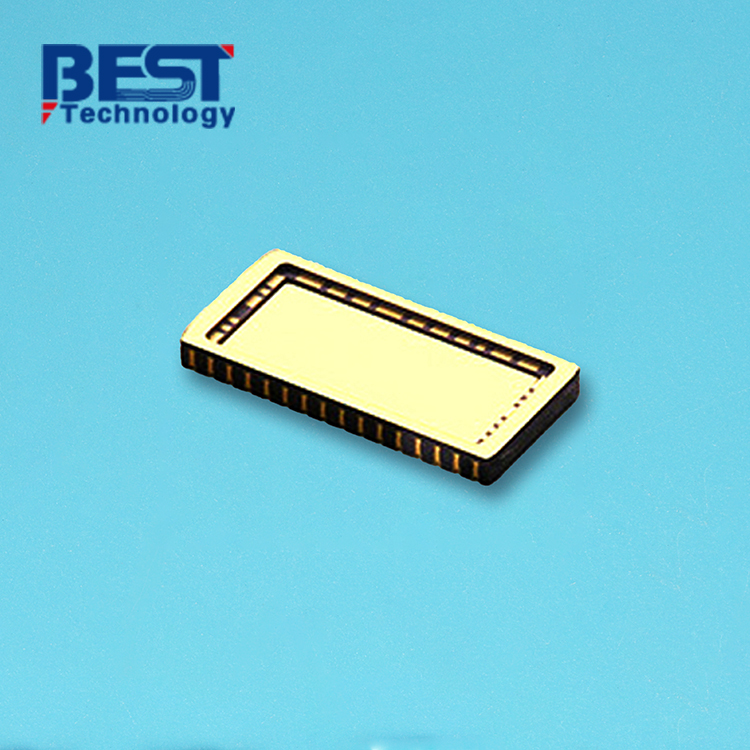
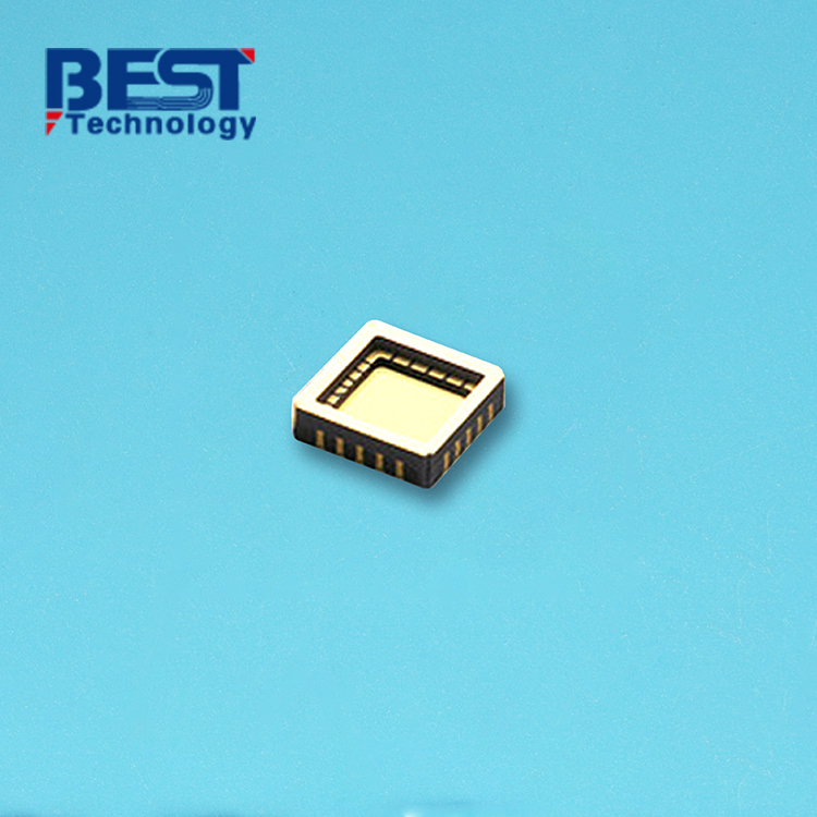
HTCC stands for High-Temperature Co-fired Ceramic. It is a type of ceramic circuit board that is widely used in high-temperature and harsh-environment applications. HTCC circuit boards offer excellent electrical performance, mechanical strength, and thermal stability, making them suitable for various industries such as aerospace, automotive, telecommunications, and power electronics.
1. Material: Al2O3, AIN
2. Function: HTCC boards can be manufactured with complex 3D structures, allowing for the integration of multiple components, such as resistors, capacitors, and even microelectromechanical systems (MEMS), within a single package. This compact integration saves space and simplifies assembly.
3. Type: Co-fired technology.
4. Custom service available.
Background:
ArtilleryTech Solutions is a leading provider of advanced artillery tactical data systems for military applications. They required a reliable and high-performance PCB solution for their systems, which involved processing and transmitting critical data in highly demanding field environments. ArtilleryTech Solutions faced several challenges in their artillery tactical data systems, including the need for rugged and reliable PCBs capable of withstanding extreme temperatures, vibrations, and mechanical shocks. They also required high-speed signal transmission, excellent signal integrity, and resistance to electromagnetic interference (EMI) to ensure accurate and secure data processing.
Solution:
After understanding the needs and challenges of ArtilleryTech faced, we recommended to use HTCC ceramic PCB as the chips, since HTCC ceramic PCB is made in very high temperature, so it can withstand the extreme temperatures. By the way, HTCC ceramic PCB is a multilayer PCB, which can meet the high-density requirements and good mechanical strengthen. Once the trace layout and schematic drawing be done, we started the production immediately, with the expedite manufacturing, we finished the products in 2 weeks and delivered the PCB to customer in timely.
When got the PCBs, customers are amazing that the boards are in a good package and all the boards are defect-free after their incoming inspection, they gave us a big satisfaction.
Result and Benefits:
The ceramic PCB worked well in the artillery tactical data system, ArtilleryTech appreciated our hard work and excellent service, in the next couple days, they introduced a new customer to us.

 Products
 About us
 Contact us


