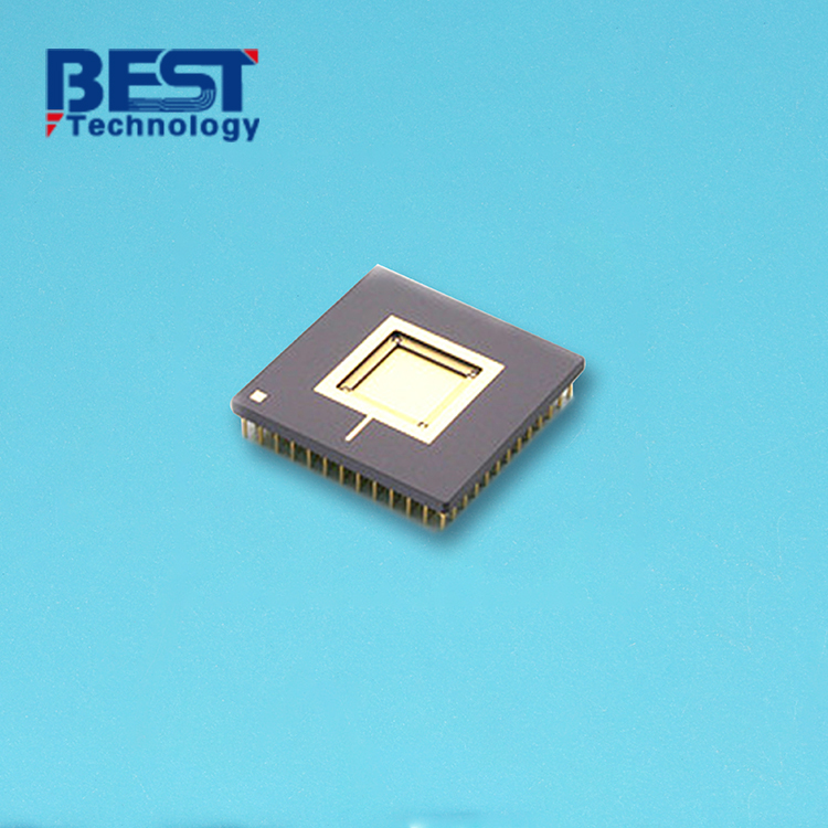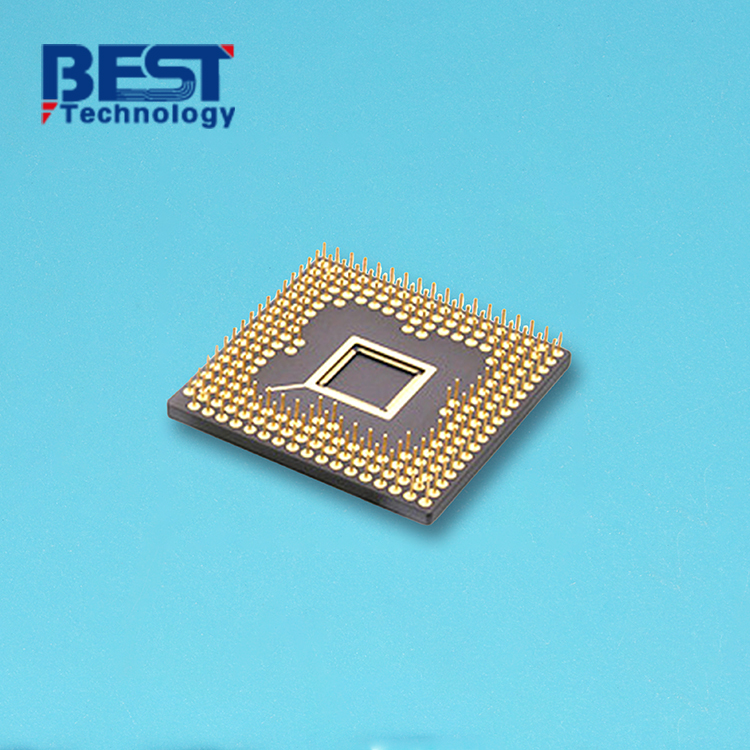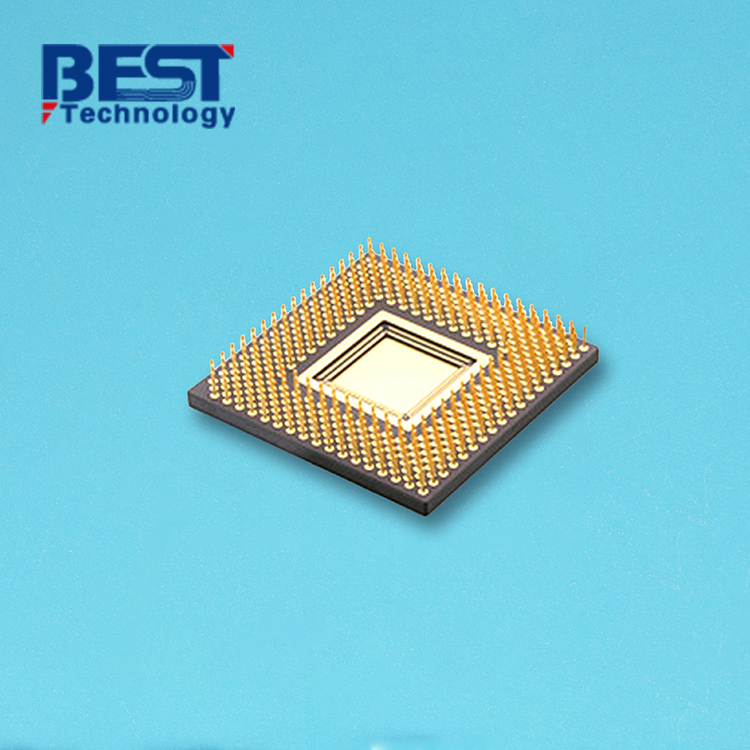
HTCC Ceramic Substrate PCB Design For Satellite Communication System


Working Temperature: -40-300℃
Conductor Thickness: 2um - 12um
LS/LW: 150um (Surface layer can be refined to 50μm)
Application: Satellite Communication System
| Item1 | HTCC Capabilities | |||||
|---|---|---|---|---|---|---|
|
Layer Count |
4-64 Layers |
|||||
|
Max Board Dimension |
150*150mm |
|||||
|
Min Board Thickness |
1Lay: 0.1mm 0.15mm |
|||||
|
Max Board Thickness |
1Lay: 0.25mm 6.0mm |
|||||
|
Conductor Thickness |
2um - 12um (Surface layer can be thickened to 80μm) |
|||||
|
Min Line Width/Line Space |
150um (Surface layer can be refined to 50μm) |
|||||
|
Substrate Type |
AI203 |
|||||
|
Substrate Thickness |
0.15-6um |
|||||
|
Min Hole Diameter |
100um |
|||||
|
Min Hole Spacing |
250um |
|||||
|
Min PAD Ring(Single) |
0.125mm |
|||||
|
PTH Wall Thickness |
No |
|||||
|
Min Solder PAD Dia |
0.1mm |
|||||
|
Min Soldermask Bridge |
75um |
|||||
|
Min BAG PAD Margin |
0.635mm |
|||||
|
PTH/NPTH Dia Tolerance |
10um |
|||||
|
Hole Position Deviation |
30-40um |
|||||
|
Outline Tolerance |
Laser: 0.005mm;Die Punch: 0.005mm |
|||||
|
Line Width/Spac Tolerance |
±20μm |
|||||
|
Surface Treatment |
Nickel-plated Gold |
|||||
|
Thermal Stress |
7.3ppm/K |
|||||
| Item2 | Attribute | ||
|---|---|---|---|
|
Brand |
CeramTec / GTT / Huaqing / Laird / Maruwa / Rogers / Toshiba |
||
|
Base Material |
AI203 |
||
|
Base Material Thickness (exclude conductor) |
0.15-6mm |
||
|
Thermal Conductivity |
17W/mk |
||
|
Soldermask Type |
AlN |
||
|
Tg Value |
800℃ |
||
|
Halogen Free |
No |
||
|
Breakdown Voltage |
15KV/mm |
||
|
Dielectric Constant (MHZ) |
9.4(1MHz) 9.1(13GHz) |
||
|
Water Absorption |
≤0.5% |
||
|
ROHS |
Yes |
||
|
Flammability |
A Level |
||
|
Thermal Conductivity (W/m.K, or W/m.C) |
17W/mk |
||
|
Dielectric Strength |
15KV/mm |
||
|
Wrap & Twist |
0.003 |
||
| Prototype(<1m²) | Layers | Normal Service | Expedited Service |
|---|---|---|---|
|
HTCC Ceramic PCB |
6 Layer |
6 - 8 weeks |
3 - 4 weeks |
|
8 Layers |
6 - 8 weeks |
3 - 4 weeks |
|
|
10 Layers |
6 - 8 weeks |
3 - 4 weeks |
|
|
Above 10 Layers |
6 - 8 weeks |
3 - 4 weeks |
| Production | Layers | Normal Service | Expedited service |
|---|---|---|---|
|
HTCC Ceramic PCB |
6 Layer |
7 - 9 weeks |
4 - 5 weeks |
|
8 Layers |
7 - 9 weeks |
4 - 5 weeks |
|
|
10 Layers |
7 - 9 weeks |
4 - 5 weeks |
|
|
Above 10 Layers |
7 - 9 weeks |
5 - 6 weeks |
HTCC Ceramic PCB vs DPC Ceramic PCB
When choosing between HTCC and DPC ceramic PCBs, it is essential to consider the specific requirements of your application and weigh them against cost considerations.
HTCC Ceramic PCB
Advantages:
Excellent heat dissipation in high-temperature environments.
Design flexibility with multilayer structures for complex circuits.
Suitable for high-frequency applications with outstanding electrical insulation.
Considerations:
Relatively higher cost compared to DPC PCBs.
Best suited for demanding scenarios and applications where thermal management and high-frequency performance are critical.
DPC Ceramic PCB
Advantages:
Cost-effective option for simpler circuits.
Provides satisfactory thermal management.
Offers good electrical insulation and supports various electronic components.
Considerations:
Not as efficient in heat dissipation as HTCC PCBs.
Limited design flexibility compared to HTCC PCBs.
Ideal for applications where cost optimization is a priority and complex circuitry is not required.
Background:
SatelliteTech Solutions required PCBs for their satellite communication systems, which operate in harsh space environments. The PCBs needed to withstand extreme temperatures, vacuum conditions, and provide reliable signal processing and transmission capabilities.
Solution:
HTCC ceramic PCBs were selected by SatelliteTech Solutions for their satellite communication systems. The HTCC ceramic PCBs provided the necessary thermal stability to endure extreme temperatures in space. Their high mechanical strength ensured resistance to mechanical stresses during launch and operation. The ceramic material's high-frequency capabilities facilitated efficient signal processing and transmission.
Result and Benefits:
The HTCC ceramic PCBs met the demanding requirements of SatelliteTech Solutions' satellite communication systems. They provided reliable signal processing and transmission, withstanding extreme temperatures and vacuum conditions. The HTCC ceramic PCBs contributed to seamless communication between satellites and ground stations, enhancing the overall performance and reliability of the satellite communication systems.


 HOME
HOME


