


 HOME
HOME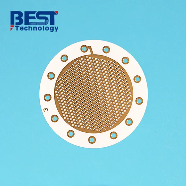
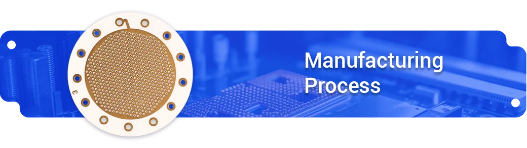
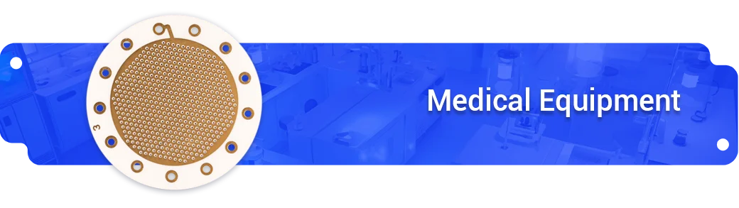
Thin Film Ceramic Circuit Board Medical Equipment Application


Board Thickness: 0.635mm
Conductor: 0.1umTi+0.2mm Pt+3.0um Au
Solder Mask: N/A
Silkscreen: N/A
Surface Finishing: N/A
Application: Medical Equipment
| Item1 | Thin Film Capabilities | Special Needs |
| Circuit layers | 1~2 Layers | N/A |
| Product Unit Size | 0.5mmx0.5mm-200mmx200mm | 0.25mmx0.25mm |
| Substrate Thickness Tolerance | ≤ ± 10% | ±0.02mm |
| Element Size Tolerance | ±0.05mm | ±0.03mm |
| Minimum Line Width@Thickness<3μm | 20μm | 10μm |
| Line Width Accuracy | ±5μm | ±2μm |
| Forecast Minimum Size Of Gold-tin Solder | 100μm*100μm | 50μm*50μm |
| Distance From Wire To Substrate Edge | 50μm | min 20μm |
| Minimum Land Size Around Vias | ≥Aperture+50μm | N/A |
| Front, Back, Multilayer Alignment Accuracy | ≤ ± 5μm | ± 1μm |
| Front, Side Alignment Accuracy | ≤ 20μm | N/A |
| Available Cutter Width | 0.1, 0.15, 0.2mm | N/A |
| Cutting Accuracy Of Grinding Wheel | ± 50μm | ± 20μm |
| Laser Cutting Precision | ± 20μm | N/A |
| Minimum Hole Diameter | 0.5*Board Thickness | N/A |
| Aperture Tolerance | ± 10% | N/A |
| Solid Hole Diameter | 0.075, 0.1mm | N/A |
| Item2 | Attributes | Special Needs |
| Brand | BSTCeramicPCB | N/A |
| Substrate type | AlN, Al2O3, Si, Quartz, Glass-ceramic, Diamond, Sapphire | N/A |
| Substrate Roughness (Ra) | ≤0.1μm | ≤0.05μm |
| Coating Type | Metal film, resistive film, dielectric film, functional film, etc. | N/A |
| Film Thickness Tolerance | ±20% | ±5% |
| Resistive film square resistance | 10-200 | N/A |
| Resistance value accuracy (laser trimmable) | ±0.1% | ±0.05% |
| Resistance value accuracy (no laser trimming) | ±5% | ±3% |
| Temperature coefficient of resistance | ±25ppm | min±10ppm |
| Rapid Prototype | Layer | Normal Delivery | Expedited Service |
| Thin Film Ceramic PCB | 1 | 3-4.5 Weeks | 2-2.5 Weeks |
| 2 | 4-6 Weeks | 2-2.5 Weeks |
| Mass Production | Layer | Normal Delivery | Expedited Service |
| Thin Film Ceramic PCB | 1 | 4-5 Weeks | 2-3 Weeks |
| 2 | 4-6 Weeks | 2-3 Weeks |
Thin film circuit boards have become one of the most crucial aspects of human life. Almost every field involves the use of thin films; this is an undeniable fact in any specific situation. Components of thin film circuitry are primarily made from non-metallic materials, providing high functionality in devices and equipment with various functions.
Thin film technology utilizes microsystem techniques and semiconductors to pave the way for circuit boards on organic or ceramic materials. The unique metal treatment process and excellent flexibility of this special technology distinguish it from printed circuit board techniques. In applications, thin film circuits possess high heat resistance, allowing them to function in situations where metals and polymers are unsuitable.
Customer Project Requirements:
MedTech Imaging Systems recently embarked on developing their next-generation medical imaging equipment, designed to provide highly accurate and detailed imaging for various medical applications. The project demanded a circuit board that could deliver exceptional precision, low noise levels, and signal accuracy, critical to obtaining clear and reliable diagnostic images.
Thin Film Ceramic PCB Application:
To meet the stringent requirements for accurate data acquisition and minimal signal interference, MedTech sought a high-performance Thin Film Ceramic PCB for their medical imaging devices. The Thin Film Ceramic PCB was expected to provide superior electrical performance, ensuring reliable data processing and minimal noise in critical medical imaging applications.
Project Challenges:
The primary challenge was to achieve extremely fine circuit patterns, maintaining low dielectric losses, and ensuring precise signal integrity while handling the high-frequency signals necessary for medical imaging devices. Additionally, the Thin Film Ceramic PCB had to comply with strict medical industry regulations for safety and performance.
Post-Project Outcome:
MedTech Imaging Systems was highly satisfied with the exceptional performance and reliability of the Thin Film Ceramic PCBs. The successful implementation of the circuit boards in their advanced medical imaging devices elevated MedTech's reputation as a pioneer in medical imaging technology. The partnership with us allowed MedTech to innovate and expand their range of medical imaging solutions, further strengthening their position in the medical equipment market.

 Products
 About us
 Contact us


