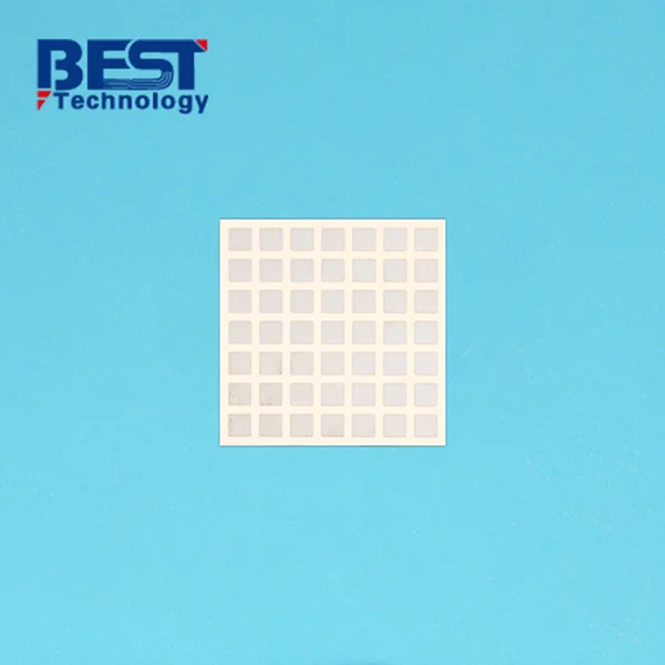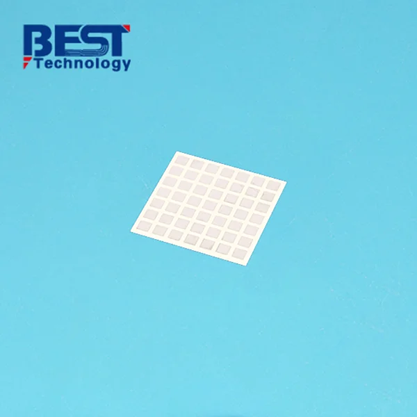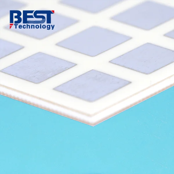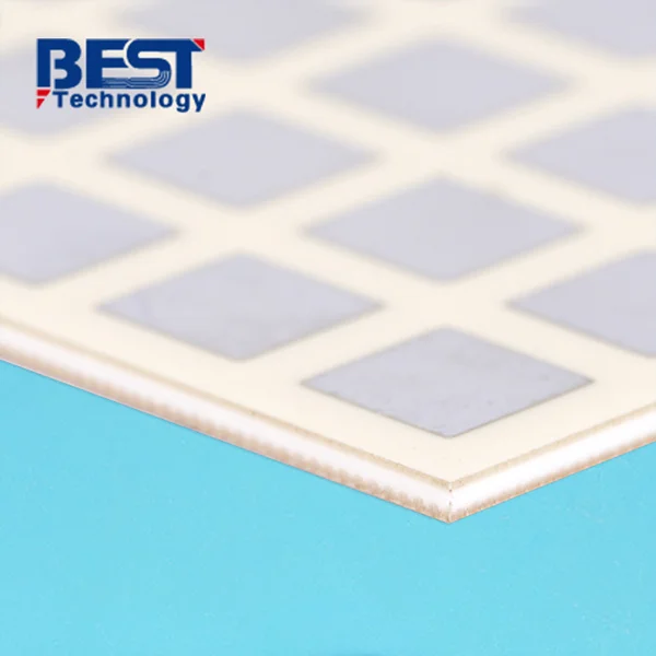
Thin-film Ceramic PCB Fast Turn Assembly For Radar Control System


Board Thickness: 1.0mm
Conductor: 0.1umTiW+3.0um Ni
Solder Mask: N/A
Silkscreen: N/A
Surface Finishing: N/A
Application: Radar System
| Item1 | Thin Film Capabilities | Special Needs |
| Circuit layers | 1~2 Layers | N/A |
| Product Unit Size | 0.5mmx0.5mm-200mmx200mm | 0.25mmx0.25mm |
| Substrate Thickness Tolerance | ≤ ± 10% | ±0.02mm |
| Element Size Tolerance | ±0.05mm | ±0.03mm |
| Minimum Line Width@Thickness<3μm | 20μm | 10μm |
| Line Width Accuracy | ±5μm | ±2μm |
| Forecast Minimum Size Of Gold-tin Solder | 100μm*100μm | 50μm*50μm |
| Distance From Wire To Substrate Edge | 50μm | min 20μm |
| Minimum Land Size Around Vias | ≥Aperture+50μm | N/A |
| Front, Back, Multilayer Alignment Accuracy | ≤ ± 5μm | ± 1μm |
| Front, Side Alignment Accuracy | ≤ 20μm | N/A |
| Available Cutter Width | 0.1, 0.15, 0.2mm | N/A |
| Cutting Accuracy Of Grinding Wheel | ± 50μm | ± 20μm |
| Laser Cutting Precision | ± 20μm | N/A |
| Minimum Hole Diameter | 0.5*Board Thickness | N/A |
| Aperture Tolerance | ± 10% | N/A |
| Solid Hole Diameter | 0.075, 0.1mm | N/A |
| Item2 | Attributes | Special Needs |
| Brand | BSTCeramicPCB | N/A |
| Substrate type | AlN, Al2O3, Si, Quartz, Glass-ceramic, Diamond, Sapphire | N/A |
| Substrate Roughness (Ra) | ≤0.1μm | ≤0.05μm |
| Coating Type | Metal film, resistive film, dielectric film, functional film, etc. | N/A |
| Film Thickness Tolerance | ±20% | ±5% |
| Resistive film square resistance | 10-200 | N/A |
| Resistance value accuracy (laser trimmable) | ±0.1% | ±0.05% |
| Resistance value accuracy (no laser trimming) | ±5% | ±3% |
| Temperature coefficient of resistance | ±25ppm | min±10ppm |
| Rapid Prototype | Layer | Normal Delivery | Expedited Service |
| Thin Film Ceramic PCB | 1 | 3-4.5 Weeks | 2-2.5 Weeks |
| 2 | 4-6 Weeks | 2-2.5 Weeks |
| Mass Production | Layer | Normal Delivery | Expedited Service |
| Thin Film Ceramic PCB | 1 | 4-5 Weeks | 2-3 Weeks |
| 2 | 4-6 Weeks | 2-3 Weeks |
Thin-film ceramic PCB, also known as microstrip ceramic PCBs, are a type of electronic substrate that utilizes thin-film technology on a ceramic surface. These boards offer several advantages over traditional thick-film ceramic PCBs. The thin-film process allows for precise control of circuit characteristics, resulting in superior high-frequency performance and reduced signal losses. This makes them an excellent choice for applications requiring RF/microwave functionality. Additionally, thin-film ceramic PCBs can achieve higher integration densities, enabling the creation of miniaturized electronic devices. However, the complexity of the manufacturing process and the need for specialized equipment make thin-film ceramic PCBs more expensive to produce, limiting their widespread use to specific high-performance applications in industries such as telecommunications, aerospace, and military.
Clients' Background:
AeroTech Avionics Inc. is an aerospace technology company specializing in avionics systems and communication solutions for aircraft and aerospace applications. With a focus on innovation and safety, AeroTech provides one-stop solutions to global aviation clients.
Customer Project Requirements:
AeroTech Avionics was developing a state-of-the-art radar system for commercial aircraft, requiring a high-frequency circuit board to support advanced communication and navigation capabilities. The project demanded a reliable and precise circuit board to ensure seamless and secure communication between aircraft and ground stations. Aerptech reached out to us to meet the stringent requirements for high-frequency communication for their radar system. The Thin Film Ceramic PCB is needed to deliver exceptional electrical performance and signal integrity to handle critical aviation communication and navigation signals.
Project Challenges:
The primary challenge was to achieve ultra-thin conductive layers with precise circuitry to enable high-frequency operation. The circuit board had to withstand the rigorous environmental conditions of aviation, including extreme temperatures, pressure, and vibration, while maintaining reliability.
Achievements:
AeroTech Avionics collaborated with us, successfully producing sample boards that surpassed performance expectations. The Thin Film Ceramic PCBs delivered exceptional electrical performance and signal integrity in aviation communication and navigation systems. The successful integration of the Thin Film Ceramic PCBs into their radar system further enhanced AeroTech's reputation as a trusted avionics technology provider. The partnership with Best Tech enabled customers to explore new opportunities in the aerospace industry, securing projects with other aviation clients seeking reliable and high-performance avionics solutions.


 HOME
HOME


