


 HOME
HOME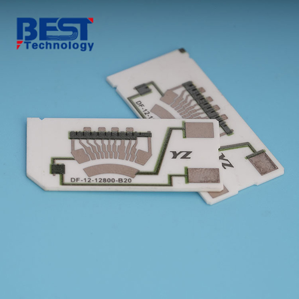
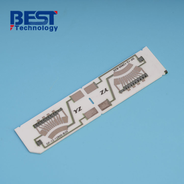
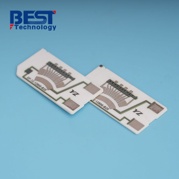
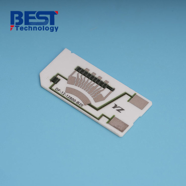
Thick Film Ceramic Substate PCB For Automotive Oil Level Sensor


Substrate Material: 96% Al2O3
Board Thickness: 0.835mm+/-0.1mm
Conductor: 10-15um AgPd
Solder Mask: Green Glass Glaze
Silkscreen: N/A
Application: Automotive Oil Level Sensor
| Item1 | Thick Film Capabilities | |||||
|---|---|---|---|---|---|---|
|
Layer Count |
1-8 Layers |
|||||
|
Max Board Dimension |
120mm×180mm |
|||||
|
Min Board Thickness |
0.254mm |
|||||
|
Max Board Thickness |
2.0mm |
|||||
|
Conductor Thickness |
7-20μm |
|||||
|
Min Line Width/Line Space |
125/150μm |
|||||
|
Substrate Type |
AIN & Si3N4 |
|||||
|
Substrate Thickness |
0.254~1.0mm |
|||||
|
Min Hole Diameter |
0.10mm |
|||||
|
Min Hole Spacing |
300μm |
|||||
|
Min PAD Ring(Single) |
0.25mm |
|||||
|
PTH Wall Thickness |
8-20um |
|||||
|
Min Solder PAD Dia |
0.25mm |
|||||
|
Min Soldermask Bridge |
150μm |
|||||
|
Min BAG PAD Margin |
0.25mm |
|||||
|
PTH/NPTH Dia Tolerance |
0.075mm |
|||||
|
Hole Position Deviation |
75μm |
|||||
|
Outline Tolerance |
Laser: +/-0.13mm |
|||||
|
Line Width/Spac Tolerance |
±20% |
|||||
|
Surface Treatment |
AgPt, AgPd, Au |
|||||
|
Thermal Stress |
7.3ppm/K |
|||||
| Item2 | Attribute | ||
|---|---|---|---|
|
Brand |
CeramTec / GTT / Huaqing / Laird / Maruwa / Rogers / Toshiba |
||
|
Base Material |
AI203 / ALN / BeO / SiO2 |
||
|
Base Material Thickness (exclude conductor) |
0.45-2.7mm |
||
|
Thermal Conductivity |
24w / 27w / 170w |
||
|
Soldermask Type |
Aluminum Nitride |
||
|
Tg Value |
800℃ |
||
|
Halogen Free |
No |
||
|
Breakdown Voltage |
>15KV/mm |
||
|
Dielectric Constant (MHZ) |
9.4 (1MHz); 9.1 (13GHz) |
||
|
Water Absorption |
≤0.5% |
||
|
ROHS |
Yes |
||
|
Flammability |
Grade A |
||
|
Thermal Conductivity (W/m.K, or W/m.C) |
24-170W/mk |
||
|
Dielectric Strength |
15KV/mm |
||
|
Wrap & Twist |
3% |
||
| Prototype(<1m²) | Layers | Normal Service | Expedited Service |
|---|---|---|---|
|
Thick Film Ceramic PCB |
1 Layer |
3 - 3.5weeks |
1-1.5 weeks |
|
2 Layers |
3 - 4 weeks |
1-1.5 weeks |
|
|
4 Layers |
3 - 4 weeks |
1-1.5 weeks |
|
| 6 Layers | 3 - 4 weeks | 1-1.5 weeks | |
| 8 Layers | 3 - 4 weeks | 1.5-2 weeks |
| Production | Layers | Normal Service | Expedited service |
|---|---|---|---|
|
Thick Film Ceramic PCB |
1 Layer |
3 - 3.5 weeks |
2 - 2.5 weeks |
|
2 Layers |
3 - 4 weeks |
2 - 2.5 weeks |
|
|
4 Layers |
3 - 4 weeks |
2 - 2.5 weeks |
|
| 6 Layers | 4 - 5 weeks | 2 - 2.5 weeks | |
| 8 Layers | 4 - 6 weeks | 2 - 2.5 weeks |
Thick film ceramic PCB refers to a type of printed circuit board that incorporates a conductor layer with a relatively thick thickness, typically exceeding 10 microns (um). This thickness is greater than what is typically achieved through other methods like thin film deposition. However, it is still less than the thickness found in DCB (Direct Copper Bonding) ceramic boards or FR4 boards.
The thick-film ceramic PCBs are utilized in a wide range of applications, including high-power LED systems, automotive components, sensors, telecommunication devices, and power electronics. Their unique properties, such as high power handling, reliability, and customization options, make them a suitable choice for demanding electronic designs across various industries.
Background:
Intercone electronics is a telecommunications medium-sized enterprise specializing in the development and manufacturing of high-frequency communication systems. Their products range from wireless routers to advanced network infrastructure equipment. In the digital age, the demand for faster and more reliable communication systems continues to grow. The customer faced challenges such as signal interference, heat dissipation, and signal loss, which affected the overall performance and reliability of their products. Meanwhile, they encountered several challenges in their communication systems. Traditional PCB materials struggled to provide the necessary thermal management, leading to heat-related failures and reduced signal integrity. Additionally, the limitations of standard PCB substrates posed obstacles in achieving high-frequency operation and efficient signal transmission. To address these issues, they turned to thick film ceramic boards as a potential solution.
Solution:
Due to the low dielectric loss and high signal transmission needed, we recommend the aluminum oxide material for the ceramic PCB, and developed a customized ceramic circuit layout according to the customer’s requirements. The thick film ceramic boards were designed to optimize signal transmission and thermal management, enabling improved performance and reliability. The unique material composition and layout minimized signal loss, enhanced signal integrity, and effectively dissipated heat, resulting in more efficient and durable communication systems.
The implementation of thick film ceramic boards had a significant impact on the customer's communication systems. The improved thermal management capabilities prevented heat-related failures and extended the lifespan of their products. Enhanced signal integrity and reduced signal loss led to better overall performance and increased customer satisfaction.
Result and Benefits:
When apply the ceramic PCB into the customer's wireless router, it demonstrated higher stability, faster data transfer rates, and improved signal reliability. Customer praise that we did a good job for them, and now we are working together on a new wire router project.

 Products
 About us
 Contact us


