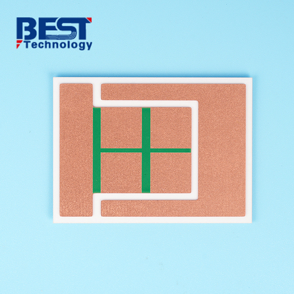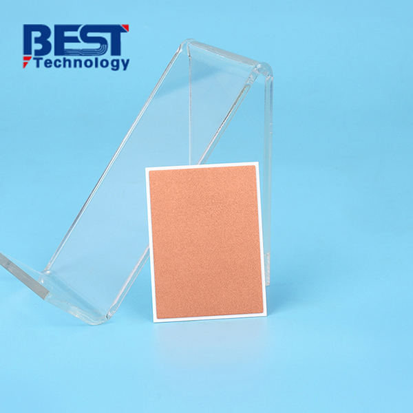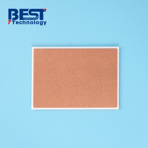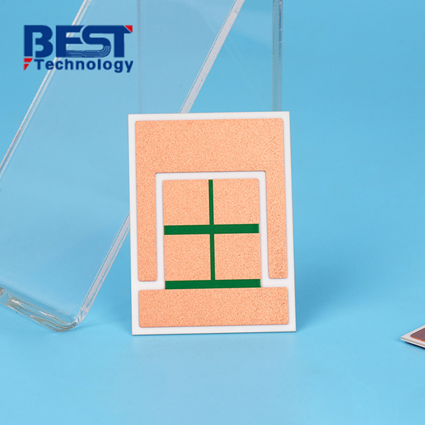
Direct Bonding Copper Ceramic Circuit Board For Automotive Components


Board Thickness: 0.635mm+/-0.1mm
Conductor: 100um copper
Solder Mask: Green Glass Glaze
Silkscreen: N/A
Surface Finishing: ENEPIG 3u’’
Application: Automotive Components
| Item1 | DCB/DBC Capabilities | |||||
|---|---|---|---|---|---|---|
|
Layer Count |
1-2 Layers |
|||||
|
Max Board Dimension |
120mmx180mm |
|||||
|
Min Board Thickness |
0.254mm |
|||||
|
Max Board Thickness |
2.0mm |
|||||
|
Conductor Thickness |
100-600μm |
|||||
|
Min Line Width/Line Space |
300/300μm |
|||||
|
Substrate Type |
AI2O3 |
|||||
|
Substrate Thickness |
0.254-2.0mm |
|||||
|
Min Hole Diameter |
0.25mm (No Via Hole) |
|||||
|
Min Hole Spacing |
250μm |
|||||
|
Min PAD Ring(Single) |
0.125mm |
|||||
|
PTH Wall Thickness |
N/A |
|||||
|
Min Solder PAD Dia |
0.5mm |
|||||
|
Min Soldermask Bridge |
Green Oil 130μm; Others 150μm |
|||||
|
Min BAG PAD Margin |
0.35mm |
|||||
|
PTH/NPTH Dia Tolerance |
0.075mm |
|||||
|
Hole Position Deviation |
75μm |
|||||
|
Outline Tolerance |
Laser: +/-0.13mm |
|||||
|
Line Width/Spac Tolerance |
±20% |
|||||
|
Surface Treatment |
OSP/Immersion Gold/Nickel Plated Gold/Immersion Silver/Nickel Plated |
|||||
|
Thermal Stress |
7.3ppm/k |
|||||
| Item2 | Attribute | ||
|---|---|---|---|
|
Brand |
CeramTec / GTT / Huaqing / Laird / Maruwa / Rogers / Toshiba |
||
|
Base Material |
AI2O3 |
||
|
Base Material Thickness (exclude conductor) |
0.45-3.2mm |
||
|
Thermal Conductivity |
24-170W/mk |
||
|
Soldermask Type |
Aluminum Oxide |
||
|
Tg Value |
800℃ |
||
|
Halogen Free |
No |
||
|
Breakdown Voltage |
>15KV/mm |
||
|
Dielectric Constant (MHZ) |
9.4 (1MHz); 9.1 (13GHz) |
||
|
Water Absorption |
≤0.5% |
||
|
ROHS |
Yes |
||
|
Flammability |
Grade A |
||
|
Thermal Conductivity (W/m.K, or W/m.C) |
24-170W/mk |
||
|
Dielectric Strength |
15KV/mm |
||
|
Wrap & Twist |
3% |
||
| Prototype(<1m²) | Layers | Normal Service | Expedited Service |
|---|---|---|---|
|
DCB/DBC Ceramic PCB |
1 Layer |
2 - 3 weeks |
1.5 weeks |
|
2 Layers |
2 - 3 weeks |
1.5 weeks |
| Production | Layers | Normal Service | Expedited service |
|---|---|---|---|
|
DCB/DBC Ceramic PCB |
1 Layer |
3 - 4 weeks |
1.5 - 2 weeks |
|
2 Layers |
3 - 4 weeks |
1.5 - 2 weeks |

In comparison to traditional PCBs that utilize substrate materials such as epoxy glass fiber, polyimide, polystyrene, and phenolic resin, ceramic PCBs possess distinct properties that make them highly desirable:
• Excellent thermal conductivity
• Chemical erosion resistant
• Agreeable mechanical intensity
• Compatible with CTE of components
• Easy to implement high-density tracing.
Due to the increasing demand for electronic devices with multiple functions, miniaturization, high speed, and larger integrated circuits (ICs), the requirements for ceramic PCBs have become more stringent. Factors such as CTE, thermal conductivity, loss, dielectric constant, and resistance to tape (solder mask) play critical roles in meeting these requirements.
DBC Ceramic PCB Specification:
|
Substrate material: |
96% Al2O3 |
|
Board thickness: |
0.635mm+/-0.1mm |
|
Conductor: |
100um copper |
|
Solder mask: |
Green Glass Glaze |
|
Silkscreen: |
N/A |
|
Surface finishing: |
ENEPIG 3u’’ |
|
Application: |
Automotive fields |
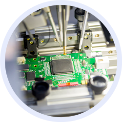 High -Power Semiconductor
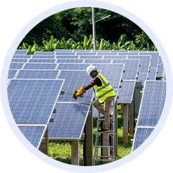 Solar Panel
 Aerospace
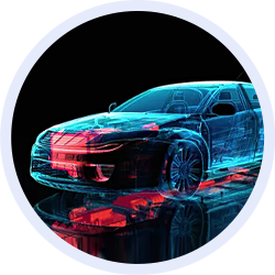 Automobile Product
 Communications Industry
 High Power LED Lighting

Background:
AcKult company is a renowned automotive parts manufacturer known for their commitment to quality and innovation. They sought to develop an electric power transmitter module capable of wirelessly transmitting power to EVs, providing a seamless and efficient charging solution. They have an initial design, but not sure this design is available and feasible, so they reached to us for evaluation and fabrication.
Project challenge:
- Due to it is for an automotive part, the quality control is very strict, it must conform to IPC Class III.
- The ceramic PCB must have a good flatness.
Solution:
To meet their objectives, we suggested to utilize DBC ceramic circuit boards made from aluminum nitride (AlN), a high-performance ceramic material known for its exceptional thermal and electrical properties. Due to the project is urgent and the deadline is on the way, we expedited the production run and finished the product in 5 days and dispatched out the ceramic PCBs in timely. AcKult team tested the PCBs immediately once receive the product and all 50pcs of them performed well and were in their expectation.
By incorporating AlN-based DBC ceramic circuit boards into their electric power transmitter modules, our client successfully developed an advanced solution for wireless power transmission in electric vehicles. These DBC ceramic circuit boards provided enhanced thermal management, excellent electrical insulation, high mechanical strength, and resistance to chemicals and corrosion. The result was a highly reliable and efficient electric power transmitter module for EV charging systems.
Result and Benefits:
Thanks to our fast fabrication and quick delivery service, AcKult team finished the task in time and they are appreciated our hard work and cooperation. Now they are one of valued customers of us.


 HOME
HOME