


 HOME
HOME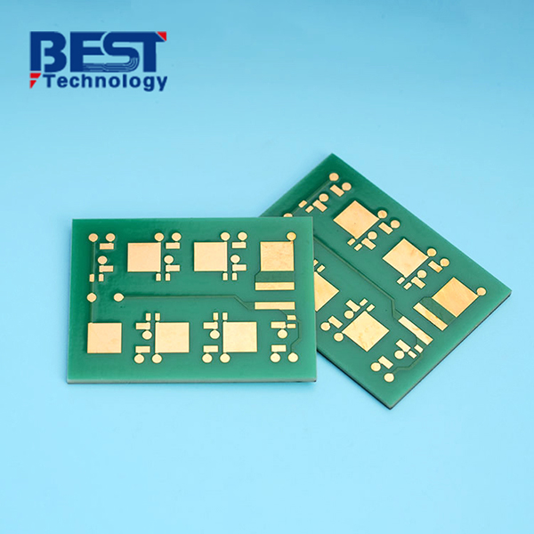
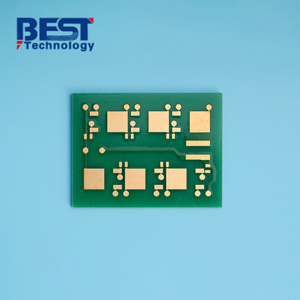
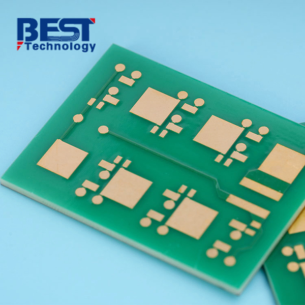
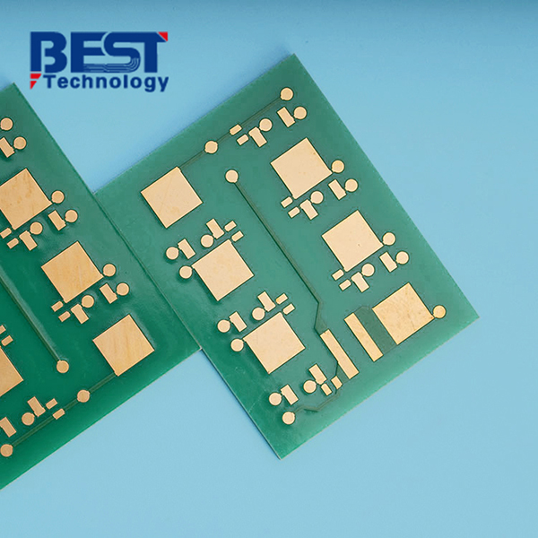
BeO Thick Film Ceramic Substrate PCB For Laser Equipment


Substrate Material: BeO
Board Thickness: 1.5mm+/-10%
Conductor: 10um AgPd + 2-5um Au
Solder Mask: Greenish Glass
Silkscreen: N/A
Application: Laser Equipment
| Item1 | Thick Film Capabilities | |||||
|---|---|---|---|---|---|---|
|
Layer Count |
1-8 Layers |
|||||
|
Max Board Dimension |
120mm×180mm |
|||||
|
Min Board Thickness |
0.254mm |
|||||
|
Max Board Thickness |
2.0mm |
|||||
|
Conductor Thickness |
7-20μm |
|||||
|
Min Line Width/Line Space |
125/150μm |
|||||
|
Substrate Type |
AIN & Si3N4 |
|||||
|
Substrate Thickness |
0.254~1.0mm |
|||||
|
Min Hole Diameter |
0.10mm |
|||||
|
Min Hole Spacing |
300μm |
|||||
|
Min PAD Ring(Single) |
0.25mm |
|||||
|
PTH Wall Thickness |
8-20um |
|||||
|
Min Solder PAD Dia |
0.25mm |
|||||
|
Min Soldermask Bridge |
150μm |
|||||
|
Min BAG PAD Margin |
0.25mm |
|||||
|
PTH/NPTH Dia Tolerance |
0.075mm |
|||||
|
Hole Position Deviation |
75μm |
|||||
|
Outline Tolerance |
Laser: +/-0.13mm |
|||||
|
Line Width/Spac Tolerance |
±20% |
|||||
|
Surface Treatment |
AgPt, AgPd, Au |
|||||
|
Thermal Stress |
7.3ppm/K |
|||||
| Item2 | Attribute | ||
|---|---|---|---|
|
Brand |
CeramTec / GTT / Huaqing / Laird / Maruwa / Rogers / Toshiba |
||
|
Base Material |
AI203 / ALN / BeO / SiO2 |
||
|
Base Material Thickness (exclude conductor) |
0.45-2.7mm |
||
|
Thermal Conductivity |
24w / 27w / 170w |
||
|
Soldermask Type |
Aluminum Nitride |
||
|
Tg Value |
800℃ |
||
|
Halogen Free |
No |
||
|
Breakdown Voltage |
>15KV/mm |
||
|
Dielectric Constant (MHZ) |
9.4 (1MHz); 9.1 (13GHz) |
||
|
Water Absorption |
≤0.5% |
||
|
ROHS |
Yes |
||
|
Flammability |
Grade A |
||
|
Thermal Conductivity (W/m.K, or W/m.C) |
24-170W/mk |
||
|
Dielectric Strength |
15KV/mm |
||
|
Wrap & Twist |
3% |
||
| Prototype(<1m²) | Layers | Normal Service | Expedited Service |
|---|---|---|---|
|
Thick Film Ceramic PCB |
1 Layer |
3 - 3.5weeks |
1-1.5 weeks |
|
2 Layers |
3 - 4 weeks |
1-1.5 weeks |
|
|
4 Layers |
3 - 4 weeks |
1-1.5 weeks |
|
| 6 Layers | 3 - 4 weeks | 1-1.5 weeks | |
| 8 Layers | 3 - 4 weeks | 1.5-2 weeks |
| Production | Layers | Normal Service | Expedited service |
|---|---|---|---|
|
Thick Film Ceramic PCB |
1 Layer |
3 - 3.5 weeks |
2 - 2.5 weeks |
|
2 Layers |
3 - 4 weeks |
2 - 2.5 weeks |
|
|
4 Layers |
3 - 4 weeks |
2 - 2.5 weeks |
|
| 6 Layers | 4 - 5 weeks | 2 - 2.5 weeks | |
| 8 Layers | 4 - 6 weeks | 2 - 2.5 weeks |
Thick-film ceramic PCBs play various roles in laser devices. But it's important to note that the specific applications and functions of thick film ceramic PCBs may vary depending on the type and design requirements of the laser device. Therefore, in practical applications, they may have more customized features and specific application areas, for example:
Power distribution: Thick film ceramic PCBs can be used for power distribution networks in laser devices. They can withstand high power currents and provide low-resistance conductive paths, ensuring efficient energy transmission and distribution.
Laser diode driving: In laser diode driver circuits, thick film ceramic PCBs can be used to provide a stable power supply and drive signals. They have excellent conductivity and thermal properties, enabling reliable power supply and drive circuits under high current conditions.
Temperature control: Laser devices often require temperature control for laser diodes and other key components. Thick film ceramic PCBs, with their good thermal conductivity and stability, can be used as heat dissipation substrates or temperature sensors to help stabilize and control the operating temperature of the device.
Sensor interfaces: In some laser devices, thick-film ceramic PCBs can be used for the fabrication of sensor interface circuits. They can provide suitable electrical interfaces and signal processing circuits for connecting and processing various sensor signals in the laser device.
Integrated circuit packaging: Thick film ceramic PCBs can be used for integrated circuit packaging, integrating key electronic components, sensors, and circuitry in laser devices. This helps reduce device size, increase integration, and provide reliable electrical connections and thermal management.
Background:
Our customer is a leading manufacturer of laser equipment, specializing in the development and production of high-performance laser systems for various industrial applications. With a focus on precision, reliability, and efficiency, they are renowned for delivering cutting-edge solutions to their clients worldwide.
The customer approached us with a specific challenge related to thermal management in their laser equipment. The high-power lasers used in their systems generate significant heat, which needs to be efficiently dissipated to ensure optimal performance and longevity. The customer sought a reliable solution that could effectively address thermal challenges while maintaining the integrity of their laser equipment.
And they want to use Beryllium Oxide for the ceramic substate material.
Project challenge:
- Material is BeO, it has long purchase period.
- Customers have strict requirements on surface cleanliness, so we should be very cautions during QC inspection.
Solution:
The application of BeO ceramic circuit boards in laser equipment has proven to be a game-changer for our customer. By leveraging the superior thermal conductivity, electrical insulation, and mechanical stability of these boards, they successfully addressed the thermal management challenges associated with high-power lasers. The integration of BeO ceramic circuit boards resulted in improved performance, reliability, and longevity of their laser equipment. As a supplier, we take pride in providing advanced solutions that enable our customers to deliver cutting-edge laser systems for diverse industrial applications.
Result and Benefits:
Customer demand was not high, but orders came in every year for a small volume, therefore, we established the long relationship with them. And this year, they sent us the assemble demand of this project for mass production.

 Products
 About us
 Contact us


