


 HOME
HOME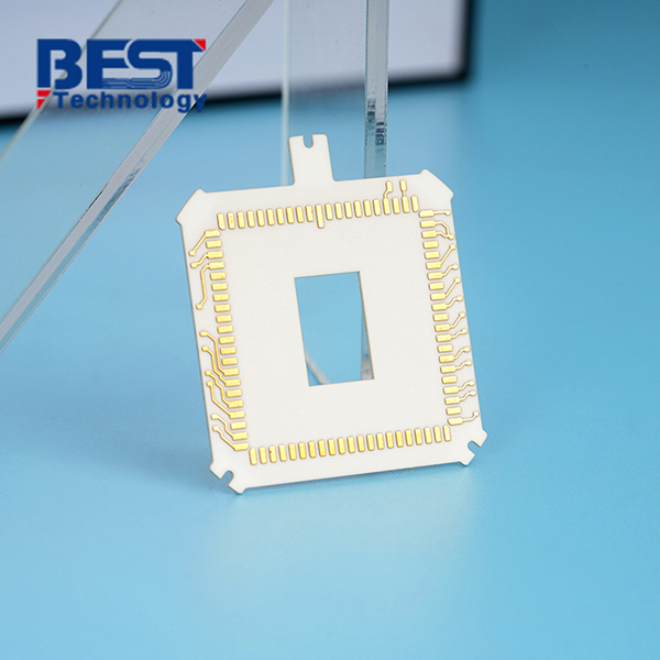
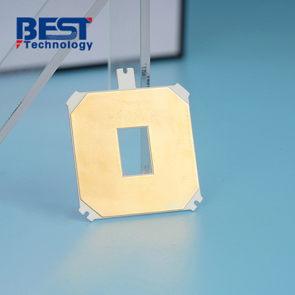
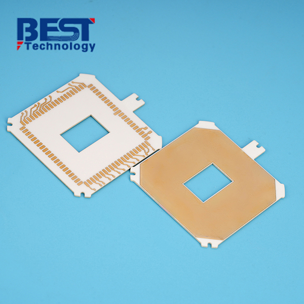
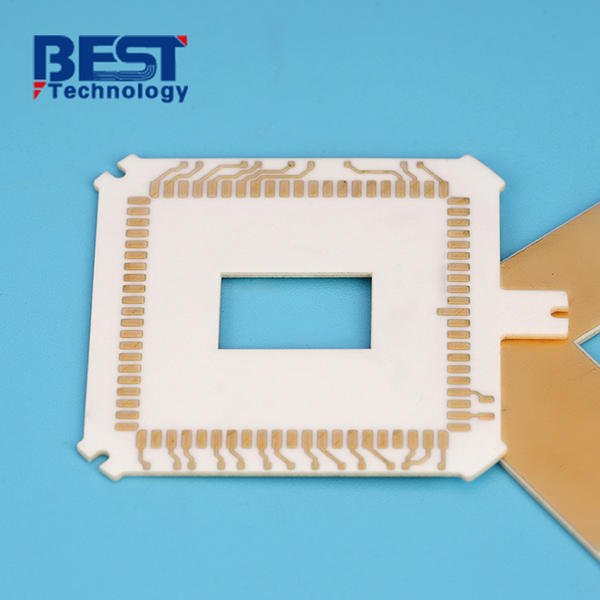
Al2O3 DPC Ceramic Substrate PCB Design For Inverter


Board thickness: 0.635mm+/-0.1mm
Conductor: 18um copper
Solder mask: N/A
Silkscreen: N/A
Surface finishing: ENEPIG 3u’’
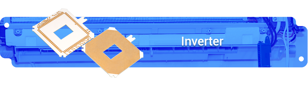
Application: Inverter
| Item1 | DPC Capabilities | |||||
|---|---|---|---|---|---|---|
|
Layer Count |
1-2 Layers |
|||||
|
Max Board Dimension |
120mmx180mm | |||||
|
Min Board Thickness |
0.15mm |
|||||
|
Max Board Thickness |
6.0mm |
|||||
|
Conductor Thickness |
50/50μm |
|||||
|
Min Line Width/Line Space |
3/3mil (0.075/0.075mm) |
|||||
|
Substrate Type |
AI2O3, ALN, Si3N4 |
|||||
|
Substrate Thickness |
0.15-6mm |
|||||
|
Min Hole Diameter |
100μm |
|||||
|
Min Hole Spacing |
250μm |
|||||
|
Min PAD Ring(Single) |
0.125mm |
|||||
|
PTH Wall Thickness |
8um |
|||||
|
Min Solder PAD Dia |
0.25mm |
|||||
|
Min Soldermask Bridge |
Green Oil 130μm; Others 150μm |
|||||
|
Min BAG PAD Margin |
0.3mm |
|||||
|
PTH/NPTH Dia Tolerance |
0.05/0.075mm |
|||||
|
Hole Position Deviation |
50-75μm |
|||||
|
Outline Tolerance |
Laser: +/-0.13mm |
|||||
|
Line Width/Spac Tolerance |
±20% |
|||||
|
Surface Treatment |
OSP/Immersion Gold/Nickel Plated Gold/Immersion Silver/Nickel Plated |
|||||
|
Thermal Stress |
7.3pmm/k |
|||||
| Item2 | Attribute | ||
|---|---|---|---|
|
Brand |
CeramTec / GTT / Huaqing / Laird / Maruwa / Rogers / Toshiba |
||
|
Base Material |
AI2O3 |
||
|
Base Material Thickness (exclude conductor) |
0.15-6mm |
||
|
Thermal Conductivity |
24-170W/mk |
||
|
Soldermask Type |
Aluminum Oxide |
||
|
Tg Value |
800℃ |
||
|
Halogen Free |
No |
||
|
Breakdown Voltage |
15 KV/mm |
||
|
Dielectric Constant (MHZ) |
9.4 (1MHz); 9.1 (13GHz) |
||
|
Water Absorption |
≤0.5% |
||
|
ROHS |
Yes |
||
|
Flammability |
Grade A |
||
|
Thermal Conductivity (W/m.K, or W/m.C) |
24-170 W/mk |
||
|
Dielectric Strength |
>15 KV/mm |
||
|
Wrap & Twist |
3% |
||
| Prototype(<1m²) | Layers | Normal Service | Expedited Service |
|---|---|---|---|
|
DPC Ceramic PCB |
1 Layer |
DPC: 2 - 3 weeks |
DPC: 1.5 weeks |
|
2 Layers |
DPC: 2 - 3 weeks |
DPC: 1.5 weeks |
| Production | Layers | Normal Service | Expedited service |
|---|---|---|---|
|
DPC Ceramic PCB |
1 Layer |
DPC: 3 - 4 weeks |
DPC: 1.5 - 2 weeks |
|
2 Layers |
DPC: 3 - 4 weeks |
DPC: 1.5 - 2 weeks |
LTCC ceramic PCBs are created by layering thin ceramic tapes, typically made of materials such as aluminum oxide (Al2O3), and then firing them at relatively low temperatures. This unique manufacturing process allows for the integration of complex three-dimensional structures, such as vias, cavities, and microchannels, within the ceramic substrate.
Heat Dissipation Comparison: Metal Core PCBs vs LTCC Ceramic PCBs
When choosing between Metal Core PCBs and LTCC Ceramic PCBs for a specific application, several factors need to be considered. Each type has its strengths and weaknesses, making them suitable for different scenarios.
Metal Core PCBs excel in high-power applications that require efficient heat dissipation and enhanced mechanical strength. They are commonly used in industries such as automotive, power electronics, and LED lighting. However, Metal Core PCBs may have limitations in terms of miniaturization and high-frequency performance.
On the other hand, LTCC Ceramic PCBs are well-suited for applications that demand both effective heat dissipation and high-frequency performance. They find applications in telecommunications, aerospace, and wireless communication systems. However, LTCC Ceramic PCBs may not be the best choice for high-power applications due to their lower thermal conductivity compared to Metal Core PCBs.
When making a decision, it is essential to consider the specific requirements of the application, including power levels, thermal management needs, and desired frequency performance.
DPC ceramic PCB specification:
|
Substrate material: |
Al2O3 |
|
Board thickness: |
0.635mm+/-0.1mm |
|
Conductor: |
18um copper |
|
Solder mask: |
N/A |
|
Silkscreen: |
N/A |
|
Surface finishing: |
ENEPIG 3u’’ |
|
Application: |
Inverter |
Background:
Innovate Electronics is a company that specializes in manufacturing Frequency converters, to improve the electrical performance and the durability of the converter, they are supposed to design a small chip that uses Aluminum oxide ceramic PCB. At present, they only have the initial Gerber file and don’t know whether it is feasible. After browsing our website, they e-mailed us and sent the files for evaluation.
PCB challenge:
The substrate thickness is too thin and it is not easy to set the laser energy, if too high the cutting-edge will become black easily.
Solution:
After checking the gerber file and understanding the end-application, our team suggested to use aluminum nitride material as the base since it has the good thermal management than aluminum oxide as well as its coefficient of thermal expansion is more closely than electronic components. In the meantime, after getting the approval from customer, we optimized the line width to smooth the production.
To overcome the black edge challenge, we fabricated the first article for laser energy evaluation, and after several experiments, we got the best energy that can ensure the edge still keep the original color and protect the edge well.
Result and Benefits:
After receiving the ceramic PCB, customer tested all the boards first and all of them passed. Then they bonded the board into the converter and found the thermal conductivity was greatly improved than previous chip, meanwhile, the durability also better than normal circuit boards. “It is really a big innovation for us”, they said, they praised our professionalism and committed that we will be the first choice if they need ceramic PCB again.

 Products
 About us
 Contact us


