


 HOME
HOMESMD
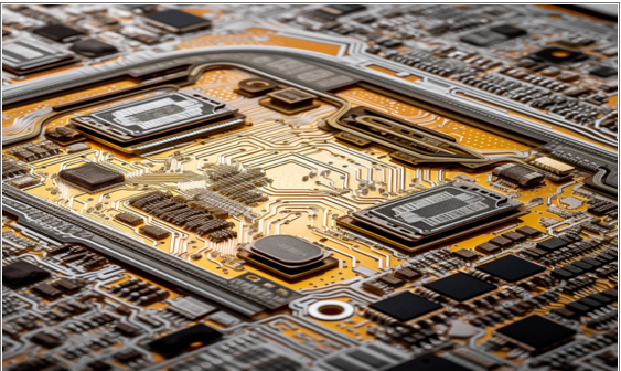
SMT technology has revolutionized the electronics industry by enabling compact and powerful devices with improved component density. It involves mounting electronic components directly onto the surface of a printed circuit board (PCB), rather than inserting them through holes as in through-hole mounting. Compared with traditional through-hole mounting, SMT technology offers several advantages during usage, including improved reliability of the circuit board, reduced board size and weight, and improved electrical performance of the whole product. This has led to the widespread adoption of SMT in various applications, including Ceramic PCBs.
The Difference Between SMD and SMT
The full name of SMT is Surface Mount Technology, while SMD is Surface Mount Device. Both two of them are often used interchangeably in sometimes, but they actually refer to two different aspects of surface mount assembly.
SMT is a method of assembling printed circuit boards (PCBs) in which electronic components are mounted directly onto the surface of the board. SMDs are electronic components that are designed to be surface-mounted and are often used in SMT assembly processes. In other words, SMT is the process and SMD is the component. SMT involves mounting various types of components, including SMDs, onto the surface of a PCB using automated assembly equipment. SMDs come in various sizes and shapes and are designed to be directly mounted onto the surface of a PCB, rather than through a hole in the board.
SMDs have several advantages over traditional through-hole components, including smaller size, lower profile, better electrical performance, and can greatly reduce assembly time and cost. SMT, as a whole, provides improved component density, enabling more compact and powerful devices.
The Importance of SMD Assembly in Ceramic PCB
SMD assembly techniques are particularly important in Ceramic PCBs, as they allow for more compact designs and improved thermal management.
Firstly, SMD assembly allows for the placement of electronic components directly onto the surface of the PCB, resulting in a higher component density and a smaller overall footprint. This is particularly important in the design of ceramic PCBs, where space is at a premium. SMD assembly also provides improved signal quality and reliability by minimizing parasitic inductance and capacitance, which can cause signal distortion and reduce the performance of high-frequency circuits.
Furthermore, SMD assembly techniques offer better solder joint quality and consistency compared to traditional through-hole mounting. With through-hole mounting, components are inserted into drilled holes on the PCB and soldered on the other side, which can lead to thermal stress and mechanical strain on the board. SMD components, on the other hand, are attached to the surface of the PCB using a reflow soldering process that ensures consistent solder joint quality and minimizes thermal stress.
SMD Assembly Techniques for Ceramic PCBs
SMD assembly techniques involve several processes, including solder paste application, component placement, and reflow soldering. Solder paste is a mixture of flux and solder particles that is applied to the PCB using a stencil. The stencil ensures that the solder paste is applied only to the required areas. Once the solder paste is applied, the components are placed on the PCB using automated equipment. The components are held in place by the solder paste, which acts as an adhesive. The PCB is then subjected to reflow soldering, which involves heating the PCB to a specific temperature to melt the solder paste and create a permanent bond between the components and the PCB.
One of the key challenges in SMD assembly on Ceramic PCBs is ensuring proper thermal management. Ceramic materials have poor thermal conductivity compared to traditional PCB materials, which can lead to heat buildup and component failure. To address this issue, SMD assembly techniques such as thermal vias and heatsinks can be used. Thermal vias are holes drilled in the PCB that allow heat to flow from the components to the other side of the PCB. Heatsinks are metal structures attached to the components that help dissipate heat.
In addition to thermal management, SMD assembly techniques in Ceramic PCBs also require careful attention to detail to ensure high reliability. Components must be placed accurately, and the solder paste must be applied precisely to prevent short circuits or open circuits. Automated inspection systems are often used to detect defects and ensure that the assembly process is consistent.
To ensure optimal performance and reliability of ceramic PCBs, it is essential to use specialized SMD assembly techniques that are specifically designed for ceramic materials. The following are some of the common SMD assembly techniques used in ceramic PCBs:
1. Laser Direct Imaging (LDI): LDI is a precise and efficient way of creating high-resolution patterns directly onto the ceramic substrate. It eliminates the need for a photomask and reduces the potential for errors caused by misalignment or dust particles.
2. Hot Air Leveling (HAL): HAL is a surface finish process that involves coating the surface of the PCB with molten solder and then using hot air to remove the excess solder, leaving a smooth and level surface for SMD components to be attached.
3. Fine Pitch Stenciling: Fine pitch stenciling involves using a specialized stencil with small openings to apply solder paste onto the ceramic substrate in a precise and uniform manner. This ensures accurate placement and optimal solder joint quality for SMD components.
4. Automated Optical Inspection (AOI): AOI is an automated process that uses high-resolution cameras to inspect the surface of the PCB for defects and errors in real-time. This ensures that any issues are identified and corrected immediately, improving the overall quality and reliability of the PCB.
SMD assembly techniques have become an essential component of the manufacturing process for ceramic PCBs. The high-frequency and high-temperature capabilities of ceramic materials require precise and efficient SMD assembly techniques to ensure optimal performance and reliability. Laser direct imaging, hot air leveling, fine pitch stenciling, and automated optical inspection are just a few of the specialized SMD assembly techniques used in the manufacturing of ceramic PCBs. By utilizing these techniques, manufacturers can produce high-quality and reliable ceramic PCBs that meet the demands of even the most demanding applications.
 Products
 About us
 Contact us


