Based on the thick film circuit technology, the metallization of the ceramic surface is achieved by magnetron sputtering, and the thickness of the copper layer is greater than 10 microns by electroplating, that is, DPC Ceramic PCB (Direct Plate Copper-direct copper plating substrate).
In terms of shape processing, DPC ceramic boards need to be cut by laser, which cannot be processed accurately by traditional drilling and milling machines and punching machines, so the bonding force and line width are also finer. The crystallization performance of the metal is good, the flatness is good, the line is not easy to fall off, and the line position is more accurate, the line distance is smaller, and the reliability is stable.
-
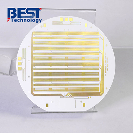
DPC Ceramic PCB Custom For New Energy Vehicles
-
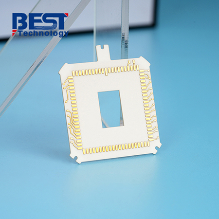
Al2O3 DPC Ceramic Substrate PCB Design For Inverter
-
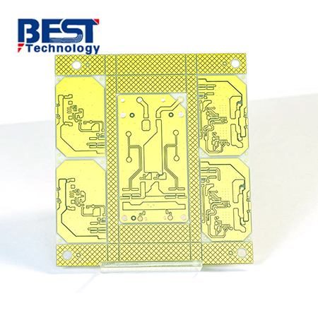
96% Al2O3 DPC Ceramic Substrate PCB Design Production For Sensor
-
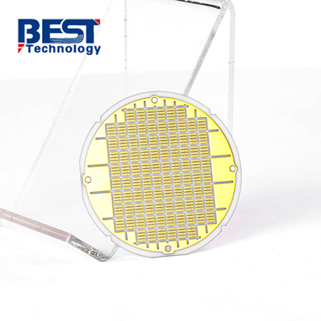
DPC Al2O3 Ceramic Substrate Circuit Board For Cooler
-
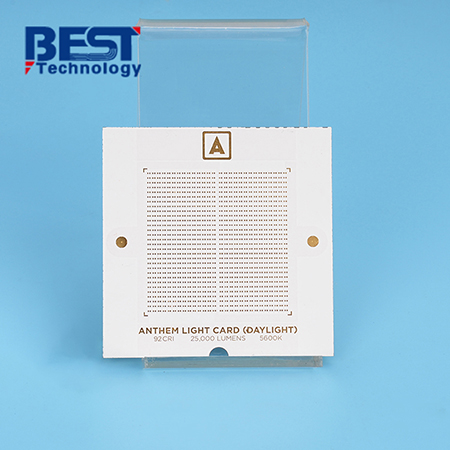
Alumina DPC Ceramic Substrate PCB Design Manufacturing For LED
-
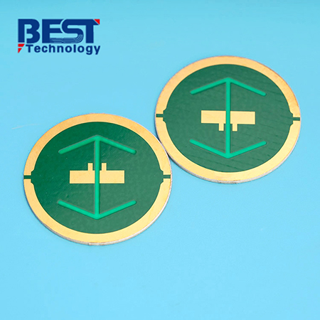
Solar Energy Application Ceramic Substrate Design AlN DPC PCB
-
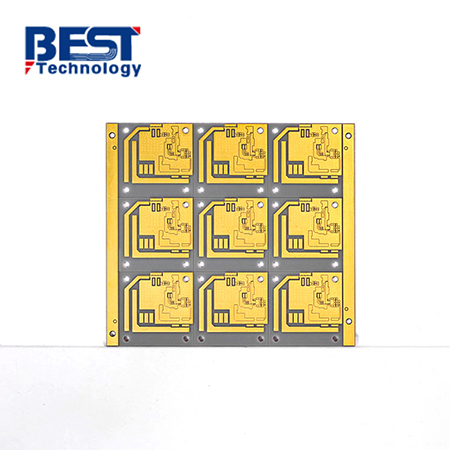
Double-sided Aluminum Nitride Filter Product DPC Ceramic Circuit Board For Stabilizer
-
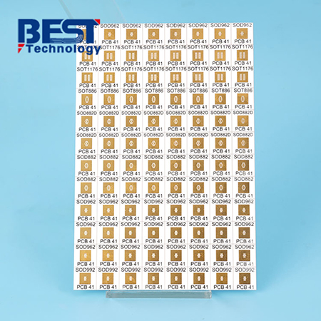
Double-sided Laser Equipment DPC Ceramic Circuit Board


 HOME
HOME


