


 HOME
HOME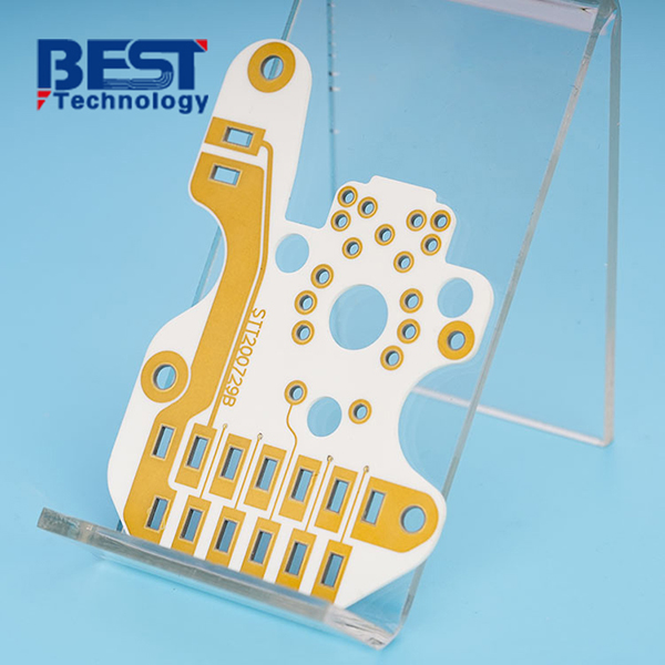
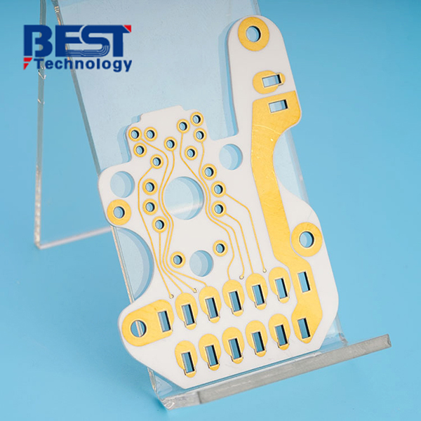
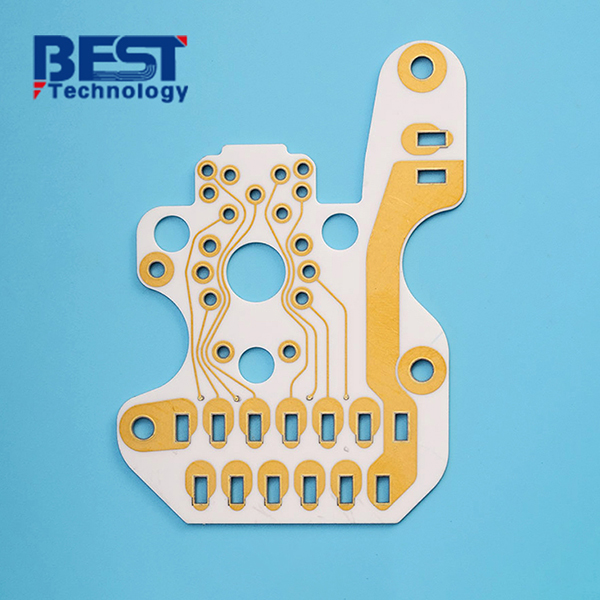
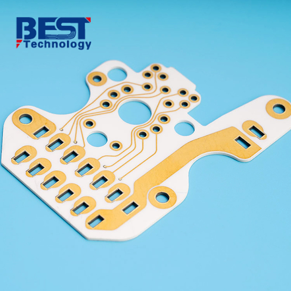
Thick Film Ceramic Substrate Double-side Circuit Board For Aerospace


Substrate Material: 96% Al2O3
Board Thickness: 0.635mm+/-0.1mm
Conductor: 3-5 um
Solder Mask: N/A
Silkscreen: N/A
Application: Infrared Imaging Spectrometer
| Item1 | Thick Film Capabilities | |||||
|---|---|---|---|---|---|---|
|
Layer Count |
1-8 Layers |
|||||
|
Max Board Dimension |
120mm×180mm |
|||||
|
Min Board Thickness |
0.254mm |
|||||
|
Max Board Thickness |
2.0mm |
|||||
|
Conductor Thickness |
7-20μm |
|||||
|
Min Line Width/Line Space |
125/150μm |
|||||
|
Substrate Type |
AIN & Si3N4 |
|||||
|
Substrate Thickness |
0.254~1.0mm |
|||||
|
Min Hole Diameter |
0.10mm |
|||||
|
Min Hole Spacing |
300μm |
|||||
|
Min PAD Ring(Single) |
0.25mm |
|||||
|
PTH Wall Thickness |
8-20um |
|||||
|
Min Solder PAD Dia |
0.25mm |
|||||
|
Min Soldermask Bridge |
150μm |
|||||
|
Min BAG PAD Margin |
0.25mm |
|||||
|
PTH/NPTH Dia Tolerance |
0.075mm |
|||||
|
Hole Position Deviation |
75μm |
|||||
|
Outline Tolerance |
Laser: +/-0.13mm |
|||||
|
Line Width/Spac Tolerance |
±20% |
|||||
|
Surface Treatment |
AgPt, AgPd, Au |
|||||
|
Thermal Stress |
7.3ppm/K |
|||||
| Item2 | Attribute | ||
|---|---|---|---|
|
Brand |
CeramTec / GTT / Huaqing / Laird / Maruwa / Rogers / Toshiba |
||
|
Base Material |
AI203 / ALN / BeO / SiO2 |
||
|
Base Material Thickness (exclude conductor) |
0.45-2.7mm |
||
|
Thermal Conductivity |
24w / 27w / 170w |
||
|
Soldermask Type |
Aluminum Nitride |
||
|
Tg Value |
800℃ |
||
|
Halogen Free |
No |
||
|
Breakdown Voltage |
>15KV/mm |
||
|
Dielectric Constant (MHZ) |
9.4 (1MHz); 9.1 (13GHz) |
||
|
Water Absorption |
≤0.5% |
||
|
ROHS |
Yes |
||
|
Flammability |
Grade A |
||
|
Thermal Conductivity (W/m.K, or W/m.C) |
24-170W/mk |
||
|
Dielectric Strength |
15KV/mm |
||
|
Wrap & Twist |
3% |
||
| Prototype(<1m²) | Layers | Normal Service | Expedited Service |
|---|---|---|---|
|
Thick Film Ceramic PCB |
1 Layer |
3 - 3.5weeks |
1-1.5 weeks |
|
2 Layers |
3 - 4 weeks |
1-1.5 weeks |
|
|
4 Layers |
3 - 4 weeks |
1-1.5 weeks |
|
| 6 Layers | 3 - 4 weeks | 1-1.5 weeks | |
| 8 Layers | 3 - 4 weeks | 1.5-2 weeks |
| Production | Layers | Normal Service | Expedited service |
|---|---|---|---|
|
Thick Film Ceramic PCB |
1 Layer |
3 - 3.5 weeks |
2 - 2.5 weeks |
|
2 Layers |
3 - 4 weeks |
2 - 2.5 weeks |
|
|
4 Layers |
3 - 4 weeks |
2 - 2.5 weeks |
|
| 6 Layers | 4 - 5 weeks | 2 - 2.5 weeks | |
| 8 Layers | 4 - 6 weeks | 2 - 2.5 weeks |
How to Place the thick film ceramic PCB Board Orders from Best Technology?
I. Define Your Requirements: Clearly understand your custom PCB board needs, including dimensions, layers, material type, resistance requirement, and design considerations.
II. Research and Select Best Technology as Your Supplier: Choose a reputable company based on experience, reputation, certifications, manufacturing capabilities, and customer reviews.
III. Request a Quotation: Contact Best Technology and provide detailed information to receive competitive pricing based on your requirements.
IV. Review Design Guidelines and Technical Support: Utilize the manufacturer's design guidelines and seek technical support to optimize your PCB board design.
V. Approve Prototypes and Conduct Testing: Evaluate prototypes for design compliance and conduct thorough testing, providing feedback for necessary improvements.
VI. Place the Final Order: Once satisfied with prototypes and testing, finalize the order details, production schedule, shipping, and payment terms while maintaining communication with the manufacturer.
Background:
DeepNan Electronics specializes in developing advanced remote-sensing instruments for space missions. Recently their engineering team is working on a project to develop an infrared imaging spectrometer for satellite-based observations of Earth's atmosphere.
In this case, thick film ceramic circuit boards will be utilized in the construction of the infrared imaging spectrometer. The spectrometer consists of multiple components, including infrared detectors, signal processing units, and data acquisition systems. The ceramic circuit boards are responsible for providing the electrical connections, interconnectivity, and integration of these components within the spectrometer.
Project challenge:
- The circuit board should be applied Au paste and AgPd paste on the traces.
- The shape shown in the door, is not a standard shape, and the outline tolerance is very strict, so we need to control the laser machine be more accurately.
Solution:
We know, for imaging and imaging analysis of the lunar surface, the infrared imaging spectrometer must be needed, which is controlled by a high-performance ultrasonic motor, and the motor is very small. Only 46 grams of ultrasonic motor weight is only 1/10 of the traditional motor. As the "heart" of the ultrasonic motor, piezoelectric ceramics can ensure that the electric power of the ultrasonic motor is strong and can withstand the big temperature difference of the moon. So the key part – ceramic PCB must have very good quality and can withstand high temperature, high voltage and characteristic as excellent wear resistance. After understanding the customer’s need, we took high attention to the manufacturing of the thick film board and successfully delivered the products within 2.5 weeks. After testing by customers, all the tests shown in green light and now they work well in the infrared imaging spectrometer.
Result and Benefits:
One of a partner of DeepNan has known us from the DeepNan, and they reach to us for a kind of ceramic PCB that need to work under high temperature. After evaluating and designing, the final prototype drawing has come out and now we are manufacturing the prototypes for them.

 Products
 About us
 Contact us


