


 HOME
HOME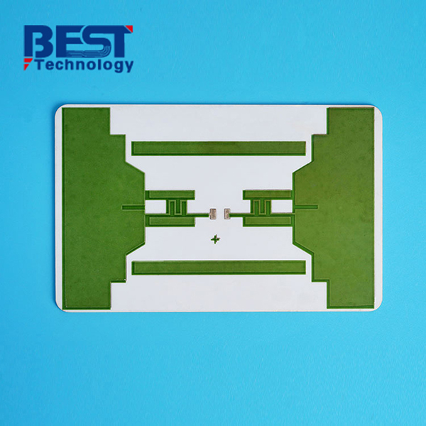
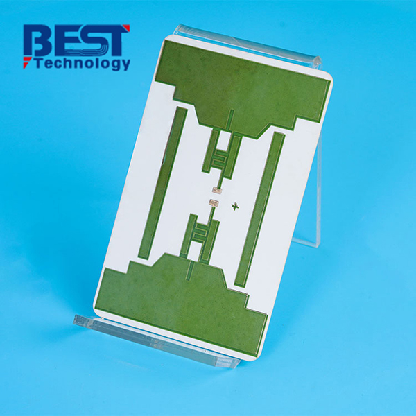
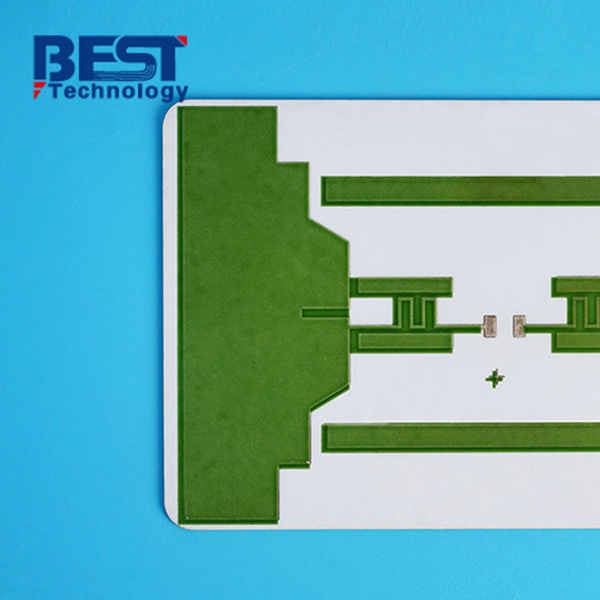
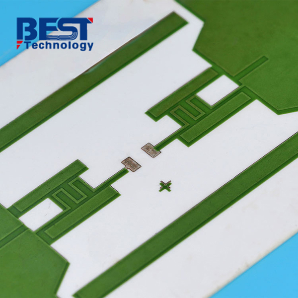
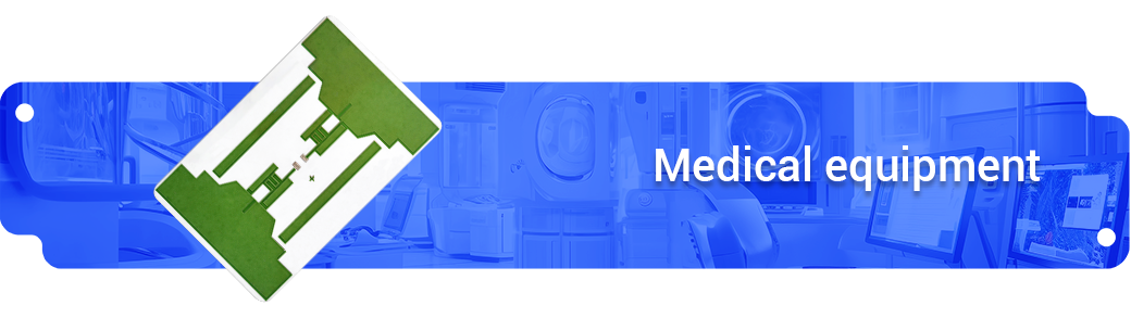
Al2O3 Thick Film Ceramic Substrate PCB For Medical Equipment


Substrate Material: 96% Al2O3
Board Thickness: 1.0mm+/-10%
Conductor: 10-15um AgPd
Solder Mask: N/A
Silkscreen: N/A
Application: Medical Equipment
| Item1 | Thick Film Capabilities | |||||
|---|---|---|---|---|---|---|
|
Layer Count |
1-8 Layers |
|||||
|
Max Board Dimension |
120mm×180mm |
|||||
|
Min Board Thickness |
0.254mm |
|||||
|
Max Board Thickness |
2.0mm |
|||||
|
Conductor Thickness |
7-20μm |
|||||
|
Min Line Width/Line Space |
125/150μm |
|||||
|
Substrate Type |
AIN & Si3N4 |
|||||
|
Substrate Thickness |
0.254~1.0mm |
|||||
|
Min Hole Diameter |
0.10mm |
|||||
|
Min Hole Spacing |
300μm |
|||||
|
Min PAD Ring(Single) |
0.25mm |
|||||
|
PTH Wall Thickness |
8-20um |
|||||
|
Min Solder PAD Dia |
0.25mm |
|||||
|
Min Soldermask Bridge |
150μm |
|||||
|
Min BAG PAD Margin |
0.25mm |
|||||
|
PTH/NPTH Dia Tolerance |
0.075mm |
|||||
|
Hole Position Deviation |
75μm |
|||||
|
Outline Tolerance |
Laser: +/-0.13mm |
|||||
|
Line Width/Spac Tolerance |
±20% |
|||||
|
Surface Treatment |
AgPt, AgPd, Au |
|||||
|
Thermal Stress |
7.3ppm/K |
|||||
| Item2 | Attribute | ||
|---|---|---|---|
|
Brand |
CeramTec / GTT / Huaqing / Laird / Maruwa / Rogers / Toshiba |
||
|
Base Material |
AI203 / ALN / BeO / SiO2 |
||
|
Base Material Thickness (exclude conductor) |
0.45-2.7mm |
||
|
Thermal Conductivity |
24w / 27w / 170w |
||
|
Soldermask Type |
Aluminum Nitride |
||
|
Tg Value |
800℃ |
||
|
Halogen Free |
No |
||
|
Breakdown Voltage |
>15KV/mm |
||
|
Dielectric Constant (MHZ) |
9.4 (1MHz); 9.1 (13GHz) |
||
|
Water Absorption |
≤0.5% |
||
|
ROHS |
Yes |
||
|
Flammability |
Grade A |
||
|
Thermal Conductivity (W/m.K, or W/m.C) |
24-170W/mk |
||
|
Dielectric Strength |
15KV/mm |
||
|
Wrap & Twist |
3% |
||
| Prototype(<1m²) | Layers | Normal Service | Expedited Service |
|---|---|---|---|
|
Thick Film Ceramic PCB |
1 Layer |
3 - 3.5weeks |
1-1.5 weeks |
|
2 Layers |
3 - 4 weeks |
1-1.5 weeks |
|
|
4 Layers |
3 - 4 weeks |
1-1.5 weeks |
|
| 6 Layers | 3 - 4 weeks | 1-1.5 weeks | |
| 8 Layers | 3 - 4 weeks | 1.5-2 weeks |
| Production | Layers | Normal Service | Expedited service |
|---|---|---|---|
|
Thick Film Ceramic PCB |
1 Layer |
3 - 3.5 weeks |
2 - 2.5 weeks |
|
2 Layers |
3 - 4 weeks |
2 - 2.5 weeks |
|
|
4 Layers |
3 - 4 weeks |
2 - 2.5 weeks |
|
| 6 Layers | 4 - 5 weeks | 2 - 2.5 weeks | |
| 8 Layers | 4 - 6 weeks | 2 - 2.5 weeks |
Using thick film technology, we can put resistor, electric capacity, conductor, semi-conductor, and interchangeable conductor on ceramic board, after manufacturing steps of printing and high-temperature sintering. We can make all the resistors with the same value, or different values for different resistors on the same board.
1. Material: Aluminum Nitride/Aluminum Oxide/Beryllium Oxide.
2. Function: The circuit board itself has resistance and no need to mount extra resistors.
3. Type: Thick film technology.
4. Custom service available.
Background:
BBA is a renowned medical device manufacturer specializing in diagnostic imaging systems. They have a strong reputation in the healthcare industry for producing advanced and reliable medical equipment. Their portfolio includes X-ray machines, CT scanners, and MRI systems.
BBA approached us to develop a custom electronic module for their latest medical imaging system. They required a high-performance circuit board capable of withstanding the demanding operating conditions and providing precise signal processing.
Thick film ceramic circuit boards were chosen for their superior thermal conductivity, excellent electrical properties, and robustness. These circuit boards are made by screen-printing multiple layers of conductive and dielectric materials onto a ceramic substrate, resulting in a dense and highly reliable electronic interconnect system.
In their expectation, the circuit boards were used in critical sections of the medical imaging system, such as the analog-to-digital converter (ADC) interface, signal amplification, and noise filtering. The precise electrical characteristics and thermal stability of the thick film ceramic circuit boards ensured accurate signal transmission and minimized interference, ultimately enhancing the image quality and diagnostic capabilities of the medical device.
Project challenge:
-
The circuit board should be applied Au paste and AgPd paste on the traces.
- The shape shows in a door, it is not a standard shape, and the outline tolerance is very strict, so we need to control the laser machine be more accurately.
Solution:
We manufactured the thick film ceramic PCB for BBA according to their gerber file within 1.5weeks and delivered to them in 3days.
Result and Benefits:
BBA is amazing to our excellent service and brilliant quality, now they have become our valued customer and placed consistent orders to us for making such PCB.

 Products
 About us
 Contact us


