


 HOME
HOME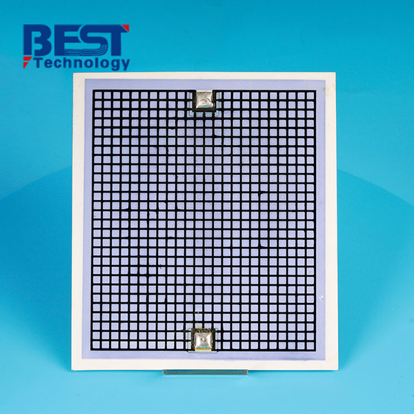
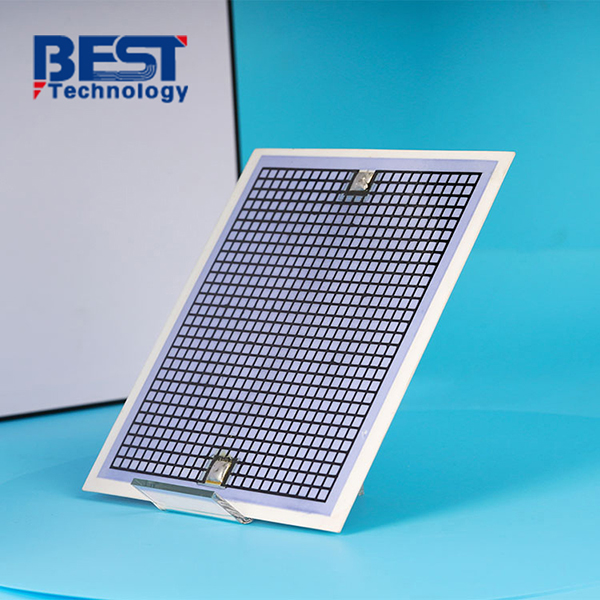
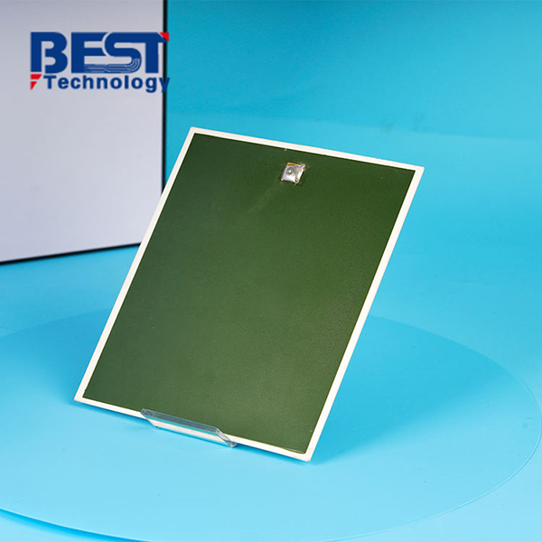
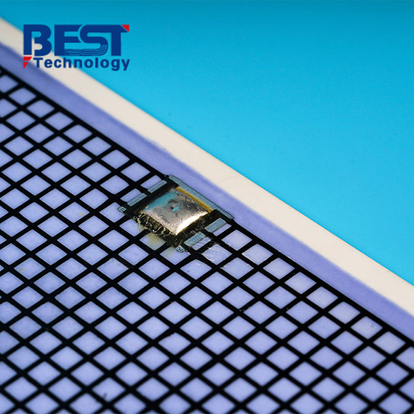
Thick Film Ceramic PCB For Ozonator


Substrate material: 96% Al2O3
Board Thickness: 1.0mm+/-10%
Conductor: 10-15um AgPd+Ru
Solder Mask: Green Glass Glaze
Silkscreen: N/A
Application: Ozonator
| Item1 | Thick Film Capabilities | |||||
|---|---|---|---|---|---|---|
|
Layer Count |
1-8 Layers |
|||||
|
Max Board Dimension |
120mm×180mm |
|||||
|
Min Board Thickness |
0.254mm |
|||||
|
Max Board Thickness |
2.0mm |
|||||
|
Conductor Thickness |
7-20μm |
|||||
|
Min Line Width/Line Space |
125/150μm |
|||||
|
Substrate Type |
AIN & Si3N4 |
|||||
|
Substrate Thickness |
0.254~1.0mm |
|||||
|
Min Hole Diameter |
0.10mm |
|||||
|
Min Hole Spacing |
300μm |
|||||
|
Min PAD Ring(Single) |
0.25mm |
|||||
|
PTH Wall Thickness |
8-20um |
|||||
|
Min Solder PAD Dia |
0.25mm |
|||||
|
Min Soldermask Bridge |
150μm |
|||||
|
Min BAG PAD Margin |
0.25mm |
|||||
|
PTH/NPTH Dia Tolerance |
0.075mm |
|||||
|
Hole Position Deviation |
75μm |
|||||
|
Outline Tolerance |
Laser: +/-0.13mm |
|||||
|
Line Width/Spac Tolerance |
±20% |
|||||
|
Surface Treatment |
AgPt, AgPd, Au |
|||||
|
Thermal Stress |
7.3ppm/K |
|||||
| Item2 | Attribute | ||
|---|---|---|---|
|
Brand |
CeramTec / GTT / Huaqing / Laird / Maruwa / Rogers / Toshiba |
||
|
Base Material |
AI203 / ALN / BeO / SiO2 |
||
|
Base Material Thickness (exclude conductor) |
0.45-2.7mm |
||
|
Thermal Conductivity |
24w / 27w / 170w |
||
|
Soldermask Type |
Aluminum Nitride |
||
|
Tg Value |
800℃ |
||
|
Halogen Free |
No |
||
|
Breakdown Voltage |
>15KV/mm |
||
|
Dielectric Constant (MHZ) |
9.4 (1MHz); 9.1 (13GHz) |
||
|
Water Absorption |
≤0.5% |
||
|
ROHS |
Yes |
||
|
Flammability |
Grade A |
||
|
Thermal Conductivity (W/m.K, or W/m.C) |
24-170W/mk |
||
|
Dielectric Strength |
15KV/mm |
||
|
Wrap & Twist |
3% |
||
| Prototype(<1m²) | Layers | Normal Service | Expedited Service |
|---|---|---|---|
|
Thick Film Ceramic PCB |
1 Layer |
3 - 3.5weeks |
1-1.5 weeks |
|
2 Layers |
3 - 4 weeks |
1-1.5 weeks |
|
|
4 Layers |
3 - 4 weeks |
1-1.5 weeks |
|
| 6 Layers | 3 - 4 weeks | 1-1.5 weeks | |
| 8 Layers | 3 - 4 weeks | 1.5-2 weeks |
| Production | Layers | Normal Service | Expedited service |
|---|---|---|---|
|
Thick Film Ceramic PCB |
1 Layer |
3 - 3.5 weeks |
2 - 2.5 weeks |
|
2 Layers |
3 - 4 weeks |
2 - 2.5 weeks |
|
|
4 Layers |
3 - 4 weeks |
2 - 2.5 weeks |
|
| 6 Layers | 4 - 5 weeks | 2 - 2.5 weeks | |
| 8 Layers | 4 - 6 weeks | 2 - 2.5 weeks |
Basic parameter of thick film ceramic PCB
-
Substrate Material: 96% or 98% Alumina (Al2O3) or Beryllium Oxide (BeO).
- Substrate Thickness: 0.25mm, 0.38mm, 0.50mm, 0.635mm (default thickness), 0.76mm, 1.0mm. Custom thicknesses like 1.6mm or 2.0mm are available.
- Conductor Layer Material: Silver palladium, gold palladium, or Mo/Mu+Ni (for Ozone).
- Conductor Layer Thickness: ≥ 10 microns (um), maximum 20 microns (0.02mm).
- Minimum Trace Width and Space (Volume Production): 0.30mm & 0.30mm. 0.20mm/0.20mm possible with increased cost. 0.15mm/0.20mm available for prototypes.
- Tolerance for Final Trace Layout: +/-10%.
- Gold Wire Bonding: Both gold and silver palladium are suitable for gold wire bonding. Special silver palladium is used for gold wire bonding upon customer request.
- Cost Considerations: Gold palladium is significantly more expensive, approximately 10-20 times higher than silver. More resistor values on the same board increase cost.
- Soldermask: Available upon request, working temperature >500°C, semi-transparent color.
Background:
EMS Electronics is a leading manufacturer of air purifiers, specializing in providing advanced solutions for clean and healthy indoor environments. With a strong focus on technological innovation and customer satisfaction, they have established themselves as a trusted brand in the air purification industry. The customer approached us with a specific challenge related to the electronic components used in their air purifiers. They required a ceramic PCB solution that could withstand the demanding conditions within the purifiers, such as exposure to airborne contaminants, high humidity, and temperature fluctuations. Additionally, they sought to enhance the overall performance and longevity of their air purification systems.
Solution:
By leveraging the benefits of thick film ceramic circuit boards and constant trials, we successfully supported our customer in developing high-performance air purifiers. The integration of advanced filtration technologies, efficient heat dissipation, and customization options enabled the customer to create innovative and reliable air purification systems. The resulting air purifiers offered improved filtration efficiency, enhanced reliability, and optimal space utilization, providing customers with clean and healthy indoor air. As a dedicated PCB supplier, we
As a dedicated PCB supplier, we take pride in delivering solutions that meet the unique needs of our customers.
Result and Benefits:
The use of our thick film ceramic circuit boards has allowed the customer to develop air purifiers that meet the highest standards of performance and reliability. This has resulted in increased customer satisfaction and loyalty. In this year, the EMS engineer and boss came to our factory and discussed the details of this project, such as the end application, the quantity demand and annual output, then placed 30,000 pieces order to us.

 Products
 About us
 Contact us


