


 HOME
HOME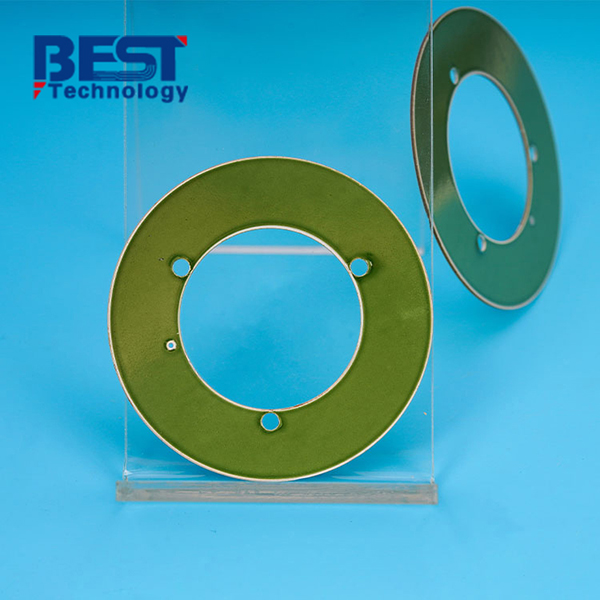
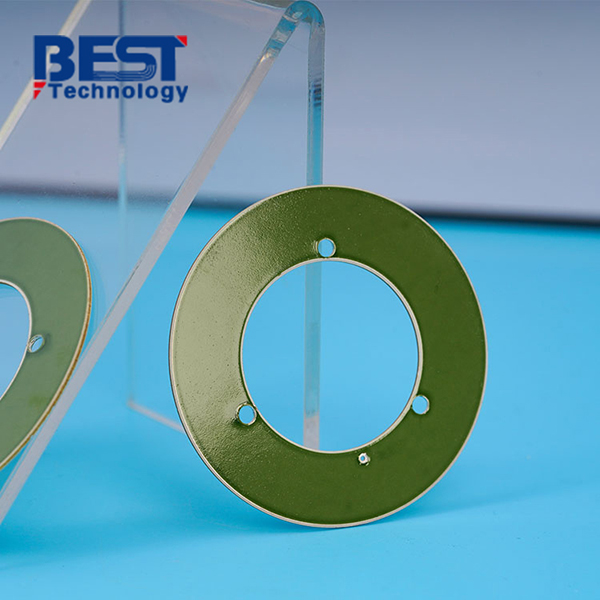
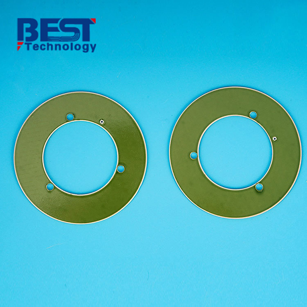
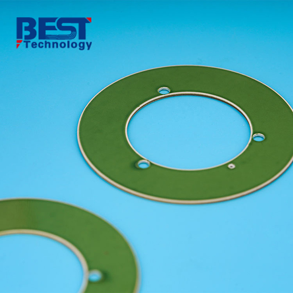
Thick Film Ceramic PCB For Scientific Research And Education Machine

 1152
1152
Substrate Material: 96% Al2O3
Board Thickness: 0.635mm+/-0.1mm
Conductor: 12-15um AgPt
Solder Mask: Greenish Glass Glaze
Silkscreen: N/A
Application: Research and Education
| Item1 | Thick Film Capabilities | |||||
|---|---|---|---|---|---|---|
|
Layer Count |
1-8 Layers |
|||||
|
Max Board Dimension |
120mm×180mm |
|||||
|
Min Board Thickness |
0.254mm |
|||||
|
Max Board Thickness |
2.0mm |
|||||
|
Conductor Thickness |
7-20μm |
|||||
|
Min Line Width/Line Space |
125/150μm |
|||||
|
Substrate Type |
AIN & Si3N4 |
|||||
|
Substrate Thickness |
0.254~1.0mm |
|||||
|
Min Hole Diameter |
0.10mm |
|||||
|
Min Hole Spacing |
300μm |
|||||
|
Min PAD Ring(Single) |
0.25mm |
|||||
|
PTH Wall Thickness |
8-20um |
|||||
|
Min Solder PAD Dia |
0.25mm |
|||||
|
Min Soldermask Bridge |
150μm |
|||||
|
Min BAG PAD Margin |
0.25mm |
|||||
|
PTH/NPTH Dia Tolerance |
0.075mm |
|||||
|
Hole Position Deviation |
75μm |
|||||
|
Outline Tolerance |
Laser: +/-0.13mm |
|||||
|
Line Width/Spac Tolerance |
±20% |
|||||
|
Surface Treatment |
AgPt, AgPd, Au |
|||||
|
Thermal Stress |
7.3ppm/K |
|||||
| Item2 | Attribute | ||
|---|---|---|---|
|
Brand |
CeramTec / GTT / Huaqing / Laird / Maruwa / Rogers / Toshiba |
||
|
Base Material |
AI203 / ALN / BeO / SiO2 |
||
|
Base Material Thickness (exclude conductor) |
0.45-2.7mm |
||
|
Thermal Conductivity |
24w / 27w / 170w |
||
|
Soldermask Type |
Aluminum Nitride |
||
|
Tg Value |
800℃ |
||
|
Halogen Free |
No |
||
|
Breakdown Voltage |
>15KV/mm |
||
|
Dielectric Constant (MHZ) |
9.4 (1MHz); 9.1 (13GHz) |
||
|
Water Absorption |
≤0.5% |
||
|
ROHS |
Yes |
||
|
Flammability |
Grade A |
||
|
Thermal Conductivity (W/m.K, or W/m.C) |
24-170W/mk |
||
|
Dielectric Strength |
15KV/mm |
||
|
Wrap & Twist |
3% |
||
| Prototype(<1m²) | Layers | Normal Service | Expedited Service |
|---|---|---|---|
|
Thick Film Ceramic PCB |
1 Layer |
3 - 3.5weeks |
1-1.5 weeks |
|
2 Layers |
3 - 4 weeks |
1-1.5 weeks |
|
|
4 Layers |
3 - 4 weeks |
1-1.5 weeks |
|
| 6 Layers | 3 - 4 weeks | 1-1.5 weeks | |
| 8 Layers | 3 - 4 weeks | 1.5-2 weeks |
| Production | Layers | Normal Service | Expedited service |
|---|---|---|---|
|
Thick Film Ceramic PCB |
1 Layer |
3 - 3.5 weeks |
2 - 2.5 weeks |
|
2 Layers |
3 - 4 weeks |
2 - 2.5 weeks |
|
|
4 Layers |
3 - 4 weeks |
2 - 2.5 weeks |
|
| 6 Layers | 4 - 5 weeks | 2 - 2.5 weeks | |
| 8 Layers | 4 - 6 weeks | 2 - 2.5 weeks |


Using thick film technology, we can put resistor, electric capacity, conductor, semi-conductor, and interchangeable conductor on ceramic board, after manufacturing steps of printing and high temperature sintering. We can make all the resistors with the same value, or different value for different resistor on the same board.
1.Material: Aluminum Nitride/Aluminum Oxide
2.Function: The circuit board itself has the resistance and no need to mount extra resistors.
3.Type: Thick film technology.
4.Custom service available.

Background:
One of our esteemed clients is a renowned research institution dedicated to pushing the boundaries of scientific discovery and promoting experiential learning. They sought to enhance their research and educational equipment by incorporating cutting-edge circuit board technology. The client faced the challenge of developing research and educational equipment with improved functionality, reliability, and versatility. They required circuit boards that could withstand demanding experimental conditions, enable precise signal processing, and support a range of scientific applications.
Project challenge:
Customer don’t have a gerber file, so we draw the drawing for them according to the requirements.
Solution:
To address their requirements, we supplied them with our high-quality thick film ceramic circuit boards. These circuit boards were designed to meet their specific needs, offering exceptional durability, excellent signal processing capabilities, and customizable design options.
By partnering with us and utilizing our thick film ceramic circuit boards, our client successfully enhanced their research and educational equipment, offering students and researchers reliable, high-performance tools. The integration of our circuit boards enabled them to conduct experiments with greater accuracy, explore complex scientific concepts, and provide hands-on learning experiences.
This case study demonstrates our commitment to delivering superior ceramic circuit board solutions that empower research and education institutions to advance scientific knowledge and foster innovation.
Result and Benefits:
Customer is amazed at our effective One-stop service, and finally we won many orders from this customer and now we have established the long relationship with them.

 Products
 About us
 Contact us


