


 HOME
HOME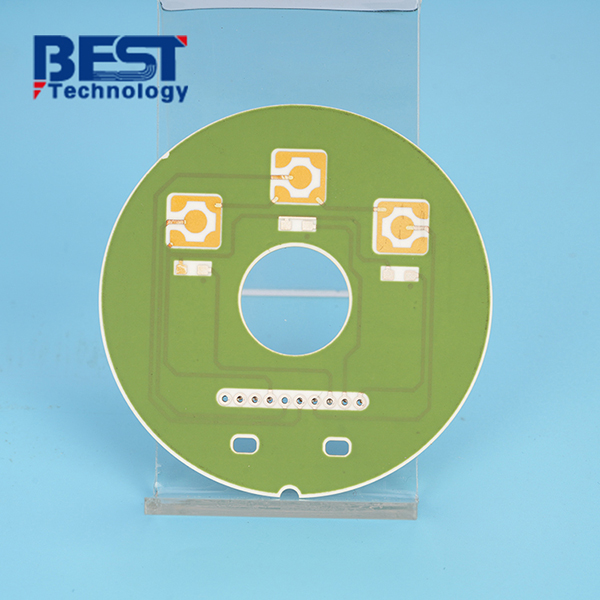
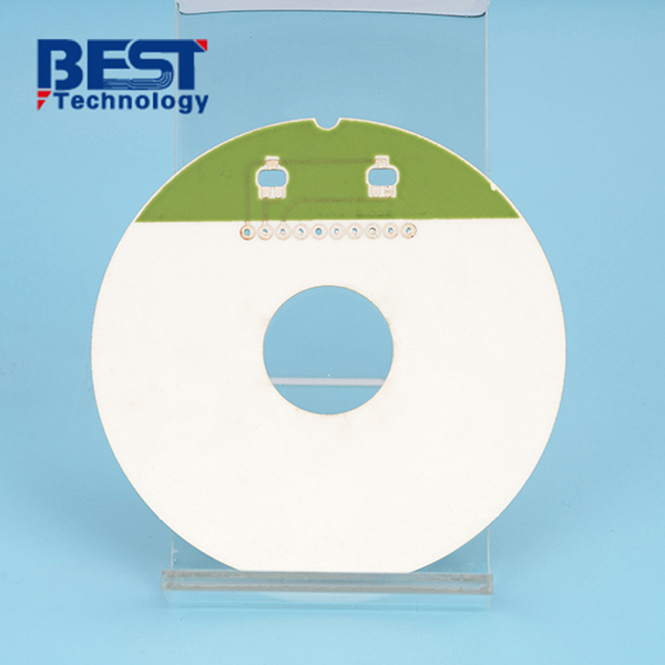
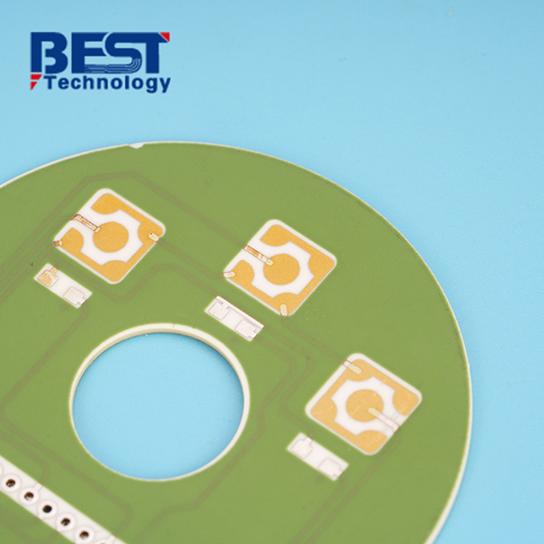
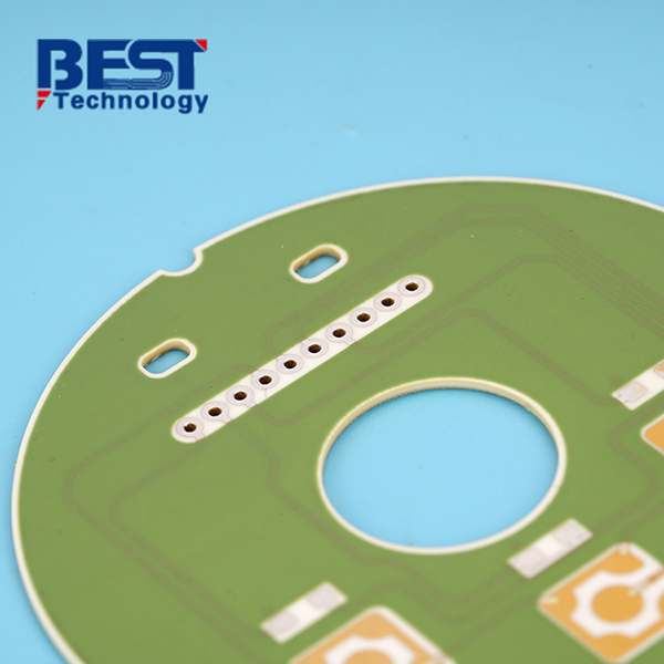
Thick Film Ceramic Substrate Board For Communication


Substrate material: 96% Al2O3
Board thickness: 0.635mm+/-0.1mm
Conductor: 10-15um AgPd-5um Au
Solder mask: Green Glass Glaze
Silkscreen: N/A
Application: Communication
| Item1 | Thick Film Capabilities | |||||
|---|---|---|---|---|---|---|
|
Layer Count |
1-8 Layers |
|||||
|
Max Board Dimension |
120mm×180mm |
|||||
|
Min Board Thickness |
0.254mm |
|||||
|
Max Board Thickness |
2.0mm |
|||||
|
Conductor Thickness |
7-20μm |
|||||
|
Min Line Width/Line Space |
125/150μm |
|||||
|
Substrate Type |
AIN & Si3N4 |
|||||
|
Substrate Thickness |
0.254~1.0mm |
|||||
|
Min Hole Diameter |
0.10mm |
|||||
|
Min Hole Spacing |
300μm |
|||||
|
Min PAD Ring(Single) |
0.25mm |
|||||
|
PTH Wall Thickness |
8-20um |
|||||
|
Min Solder PAD Dia |
0.25mm |
|||||
|
Min Soldermask Bridge |
150μm |
|||||
|
Min BAG PAD Margin |
0.25mm |
|||||
|
PTH/NPTH Dia Tolerance |
0.075mm |
|||||
|
Hole Position Deviation |
75μm |
|||||
|
Outline Tolerance |
Laser: +/-0.13mm |
|||||
|
Line Width/Spac Tolerance |
±20% |
|||||
|
Surface Treatment |
AgPt, AgPd, Au |
|||||
|
Thermal Stress |
7.3ppm/K |
|||||
| Item2 | Attribute | ||
|---|---|---|---|
|
Brand |
CeramTec / GTT / Huaqing / Laird / Maruwa / Rogers / Toshiba |
||
|
Base Material |
AI203 / ALN / BeO / SiO2 |
||
|
Base Material Thickness (exclude conductor) |
0.45-2.7mm |
||
|
Thermal Conductivity |
24w / 27w / 170w |
||
|
Soldermask Type |
Aluminum Nitride |
||
|
Tg Value |
800℃ |
||
|
Halogen Free |
No |
||
|
Breakdown Voltage |
>15KV/mm |
||
|
Dielectric Constant (MHZ) |
9.4 (1MHz); 9.1 (13GHz) |
||
|
Water Absorption |
≤0.5% |
||
|
ROHS |
Yes |
||
|
Flammability |
Grade A |
||
|
Thermal Conductivity (W/m.K, or W/m.C) |
24-170W/mk |
||
|
Dielectric Strength |
15KV/mm |
||
|
Wrap & Twist |
3% |
||
| Prototype(<1m²) | Layers | Normal Service | Expedited Service |
|---|---|---|---|
|
Thick Film Ceramic PCB |
1 Layer |
3 - 3.5weeks |
1-1.5 weeks |
|
2 Layers |
3 - 4 weeks |
1-1.5 weeks |
|
|
4 Layers |
3 - 4 weeks |
1-1.5 weeks |
|
| 6 Layers | 3 - 4 weeks | 1-1.5 weeks | |
| 8 Layers | 3 - 4 weeks | 1.5-2 weeks |
| Production | Layers | Normal Service | Expedited service |
|---|---|---|---|
|
Thick Film Ceramic PCB |
1 Layer |
3 - 3.5 weeks |
2 - 2.5 weeks |
|
2 Layers |
3 - 4 weeks |
2 - 2.5 weeks |
|
|
4 Layers |
3 - 4 weeks |
2 - 2.5 weeks |
|
| 6 Layers | 4 - 5 weeks | 2 - 2.5 weeks | |
| 8 Layers | 4 - 6 weeks | 2 - 2.5 weeks |
How Best Technology Serve You?
- Superior Ceramic Boards: Our expertise lies in producing ceramic boards with exceptional flatness and precise printed resistor values, ensuring high-quality performance for your applications.
- Custom Layout Services: We offer flexible custom layout services, tailoring the design of ceramic boards to perfectly match your specific requirements, guaranteeing optimal functionality and fit.
- Professional Technical Support: Our dedicated technical support team is here to assist you every step of the way, providing expert guidance and resolving any design or production issues promptly and efficiently.
- On-Time Delivery and Competitive Pricing: We prioritize on-time delivery to meet your project timelines and offer competitive pricing that aligns with your budget, providing excellent value for your investment.
- Stringent Quality Control: Our manufacturing takes place in a state-of-the-art, 2000-class dust-free workshop. Each production process undergoes rigorous quality control measures, ensuring the highest level of product quality and reliability.
- Quality Certifications and Traceability: We hold prestigious certifications, including ISO 9001, ISO 13485, and IATF 16949, showcasing our commitment to maintaining the highest quality standards. Our dedicated QC team diligently monitors all manufacturing processes, ensuring adherence to these standards. With comprehensive traceability measures in place, we can provide detailed data and documentation for complete transparency and accountability.
Thick Film Ceramic PCB specification:
|
Substrate material: |
96% Al2O3 |
|
Board thickness: |
0.835mm+/-10% |
|
Conductor: |
10-15um AgPd |
|
Solder mask: |
Green |
|
Silkscreen: |
N/A |
|
Surface finishing: |
N/A |
|
Application: |
Communication |
Background:
Intercone electronics is a telecommunications medium-sized enterprise specializing in the development and manufacturing of high-frequency communication systems. Their products range from wireless routers to advanced network infrastructure equipment. In the digital age, the demand for faster and more reliable communication systems continues to grow. The customer faced challenges such as signal interference, heat dissipation, and signal loss, which affected the overall performance and reliability of their products. Meanwhile, they encountered several challenges in their communication systems. Traditional PCB materials struggled to provide the necessary thermal management, leading to heat-related failures and reduced signal integrity. Additionally, the limitations of standard PCB substrates posed obstacles in achieving high-frequency operation and efficient signal transmission. To address these issues, they turned to thick film ceramic boards as a potential solution.
Solution:
Due to the low dielectric loss and high signal transmission needed, we recommend the aluminum oxide material for the ceramic PCB, and developed a customized ceramic circuit layout according to the customer’s requirements. The thick film ceramic boards were designed to optimize signal transmission and thermal management, enabling improved performance and reliability. The unique material composition and layout minimized signal loss, enhanced signal integrity, and effectively dissipated heat, resulting in more efficient and durable communication systems.
The implementation of thick film ceramic boards had a significant impact on the customer's communication systems. The improved thermal management capabilities prevented heat-related failures and extended the lifespan of their products. Enhanced signal integrity and reduced signal loss led to better overall performance and increased customer satisfaction.
Result and Benefits:
When apply the ceramic PCB into the customer's wireless router, it demonstrated higher stability, faster data transfer rates, and improved signal reliability. Customer praise that we did a good job for them, and now we are working together on a new wire router project.

 Products
 About us
 Contact us


