


 HOME
HOMEDPC PCB Assembly
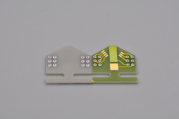
Ceramic PCB Assembly In China
Whether you need a few quick-turn prototypes or a few thousand production ceramic PCBs, BSTCeramicPCB offers one-stop ceramic PCB assembly services for your boards at the scale you need.
1. SMT assembly
2. Turnkey assembly
3. BGA/QFN assembly
4. IC programming
5. Through-hole assembly
6. Mixed assembly
7. Pin assembly
8. Ceramic circuit board assembly
9. Component package: Reels, Cut Tape, Tube, Tray, Loose Parts
We source and purchase components from chip manufacturers worldwide, including Mouser, Digi-Key, Arrow Electronics, and other suppliers. Additionally, we maintain a substantial inventory of frequently used parts in our warehouse. When a particular component is unavailable, our engineers offer suggestions for suitable alternatives at reasonable prices.
Assembly Capabilities for DPC Ceramic PCB
1. Substrate dimension: L5050MM~L510360MM
2. Chip specification: 01005 packages and above parts
3. BGA pitch: >=0.15mm with 100% 3D AOI and X-ray inspection
4. Mount accuracy: 0.05mm
5. Assembly speed: 0.04s/point
6. ROHS certificated and Lead-Free promise
7. 3D SPI detection to ensure good solderability
Assembly Process
The assembly process for DPC ceramic PCBs is similar to that of traditional PCBs, but there are specific considerations due to the unique properties of ceramic substrates. Below is a general overview of the DPC ceramic PCB assembly process:
1. Stencil preparation
2. Solder paste selection
3. Solder paste printing (key)
4. First article inspection
5. Feeder loading and components mount
6. Nitrogen reflowing temperature setting (key)
7. Reflow soldering
8. Visual inspection + 3D AOI detection
9. X-RAY detection
10. Testing
11. FQC & QA inspection
12. Package and shipment
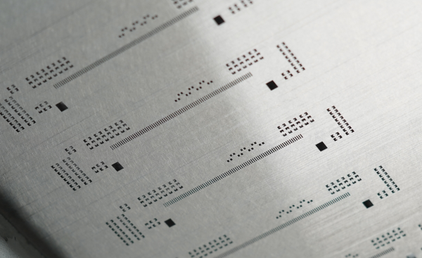
1. Stencil Preparation
Stencil often made from stainless steel, is laser-cut or chemically etched to achieve precise openings and desired pad patterns that match the solder pads on the ceramic circuit boards. Different from normal rigid PCBs, the ceramic circuit board size is very small, so the stencil printing area is relevant smaller.
On the other hand, to prevent the solder paste from spreading to the side pad, the openings generally are 80% area of the actual pad size if the ceramic PCB without a solder mask (large connector will follow 1:1 to do).
To ensure accurate and consistent solder paste printing, the stencil is cleaned and inspected for defects before use.
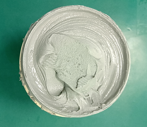
2. Solder Paste Selection
Selecting the right solder paste for DPC ceramic PCB assembly is a critical decision. Factors such as the substrate material, component types, reflow temperature profile, and desired reliability play into this choice. High-temperature-resistant solder pastes with suitable flux formulations are often favored for ceramic PCBs. The solder paste's particle size distribution, viscosity, and rheology are optimized to enable precise dispensing during printing, ensuring consistent solder joint quality. In BSTCeramicPCB, we always use SAC305 high-temperature and lead-free solder paste for ceramic PCB soldering, because it has excellent electrical conductivity and good wettability, enable to ensure good solderability.
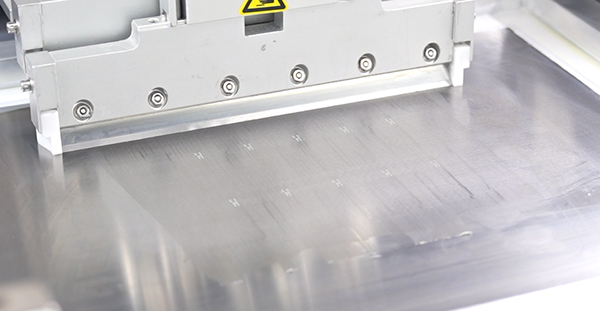
3. Solder Paste Printing (Key Process)
Solder paste printing is a critical step that directly affects the quality of solder joints and overall assembly reliability. This process is to deposit solder paste onto designated pads on the DPC ceramic substrate. Proper solder paste printing ensures consistent and reliable connections between components and the substrate during reflow soldering.
During solder paste printing:
- Precise alignment of the stencil is crucial to ensure accurate deposition of solder paste onto the pads.
- Optimal squeegee pressure and speed are set to achieve uniform and controlled solder paste application, now our advanced 3D SPI machine can solve this problem perfectly.
- Thorough 3D SPI inspection is conducted to verify that the solder paste is correctly deposited, without smearing or misalignment.
- Any defects, such as insufficient or excessive solder paste, are identified and corrected before proceeding to the next assembly step.
Achieving high-quality solder paste printing is essential to prevent issues like solder bridging, incomplete wetting, or tombstoning during reflow soldering. Rigorous process control and monitoring during this stage contribute to the overall success of the assembly process.
But there is a very important thing before solder paste printing, cleaning the substrate surface with alcohol to avoid poor solderability.
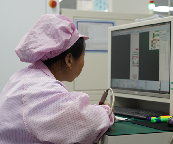
4. First Article Inspection
The first article inspection (FAI) involves a comprehensive evaluation of the initial assembly to identify any discrepancies between the actual assembly and the intended design. This step verifies proper solder paste printing, component placement accuracy, and alignment. FAI helps catch potential issues early, allowing adjustments to be made before proceeding to full-scale production. It includes both visual inspection and measurements using specialized tools to ensure that the solder paste is correctly deposited and aligned on the DPC ceramic substrate.
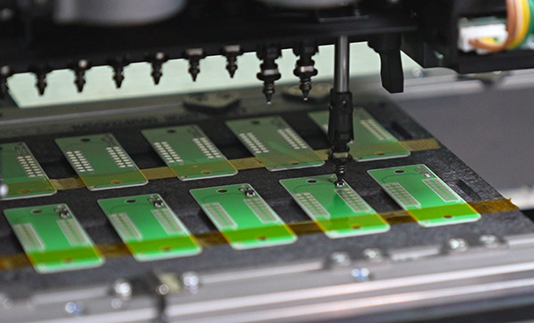
5. Feeder Loading and Component Mounting
Careful loading of feeders on the pick-and-place machine is crucial for maintaining efficient assembly. Components are carefully loaded, and machine parameters are configured to handle the specifics of DPC ceramic PCBs, which may include their fragility and unique dimensions. Component mounting is a high-precision operation, ensuring components are placed accurately and securely onto the solder paste-coated pads, aligning with the design layout.
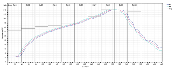
6. Nitrogen Reflowing Temperature Setting (Key Process)
The temperature setting of Nitrogen reflow soldering plays a vital role in ensuring robust and reliable solder joint formation, especially in the context of DPC ceramic PCB assembly. Nitrogen is used to create an inert atmosphere within the reflow oven, which minimizes oxidation of both solder paste and the DPC ceramic substrate.
Key considerations during nitrogen reflowing temperature setting:
- Temperature Profiles: An optimized reflow profile is established, taking into account the unique thermal properties of DPC ceramic materials. The ramp-up, soak, and cool-down phases are carefully controlled to prevent thermal stress and bubbles on the substrate.
- Nitrogen Flow Rate: The nitrogen flow rate is precisely calibrated to maintain a consistent inert environment. This prevents the formation of oxide layers on solder joints, ensuring strong intermetallic bonds.
- DPC Ceramic Compatibility: The reflow temperature must be within the safe operating range of the DPC ceramic substrate to avoid warping, cracking, or other forms of damage.
- Thermal Uniformity: Ensuring even heat distribution across the assembly is critical to prevent localized overheating or underheating, which can lead to solder joint defects.
Proper execution of this process contributes significantly to the long-term performance of the final product in demanding operational environments. At BSTCeramicPCB, we have a unique temperature setting for ceramic PCB, after continuous testing and verification, we can determine that this is the most suitable temperature for reflow soldering ceramic PCBs.
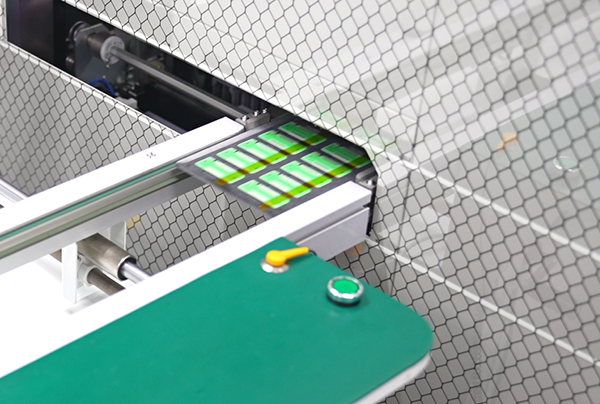
7. Reflow Soldering
Reflow soldering involves subjecting the DPC ceramic PCB assembly to a carefully controlled thermal profile in a reflow oven. The thermal profile includes gradual ramping up to reflow temperature, a controlled dwell time, and controlled cooling to solidify solder joints. For ceramic PCBs, it's crucial to account for the substrate's thermal expansion properties to prevent warping or mechanical stress. The reflow process ensures that the solder paste transitions from a paste to a liquid state and then solidifies, forming reliable interconnections between components and the DPC ceramic substrate.
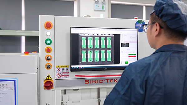
8. Visual Inspection + 3D AOI Detection
Visual inspection involves a meticulous examination of solder joints, component alignment, and overall assembly quality. Because during reflowing, we can’t ensure ceramic PCB whether happens component drop or bubbles, performing a visual inspection in this step can help to evade issues in advance. Automated Optical Inspection (AOI) systems use advanced cameras and lighting to detect defects that may not be visible to the naked eye. In 3D AOI, the system captures detailed images of the assembly from multiple angles, enabling thorough inspection of solder joint quality, component placement, and solder paste printing accuracy. Not only ceramic PCB, but all the assembled PCBAs produced by BSTCeramicPCB will also be detected by 3D AOI to confirm the good quality and no dis-alignment.
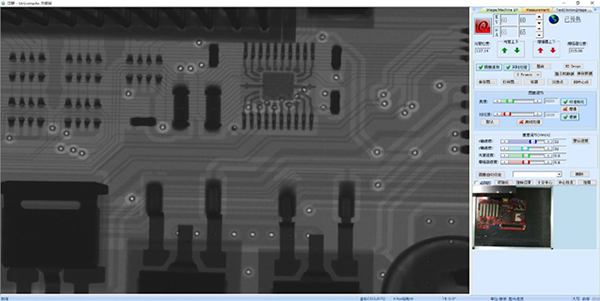
9. X-RAY Detection
X-ray inspection is a non-destructive method used to inspect hidden solder joints, such as those underneath Ball Grid Array (BGA), Quad Flat No-lead (QFN) components, IC chips or in complex package structures. X-rays penetrate the assembly, revealing internal solder joint quality and potential defects, such as voids or insufficient wetting. X-ray inspection provides valuable insights into the integrity of connections within the assembly's critical areas.
10. Testing
Testing involves subjecting the DPC ceramic PCB assembly to various electrical and functional tests. Continuity tests verify that electrical paths are intact, impedance tests ensure signal integrity and functional tests validate the performance of the assembly under specific conditions. Testing equipment is calibrated and configured to account for the unique characteristics of DPC ceramic PCBs, ensuring accurate and reliable test results.
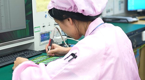
11. FQC & QA Inspection
These inspections involve a combination of visual checks, functional tests, and measurements to ensure that the assembly meets predetermined standards and specifications. FQC team generally performs full inspection including appearance inspection, components inspection and functional test, while QA teams meticulously review documentation, test results, assembly records and random inspection to verify compliance with quality standards and customer requirements. We deeply understand that quality is the core of a product, so all of our employees pay high attention to quality inspection and control.
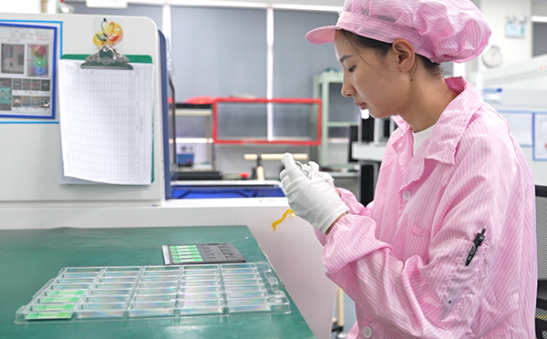
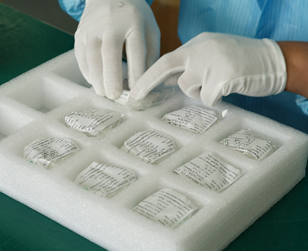
12. Package and Shipment
Due to the ceramic PCB being extremely fragile and easy to be damaged, the packaging is a critical step to protect the assembled circuit board. A rough package will cause ceramic PCBA to break or components to drop whether in transportation and storage. Specialized packaging such as blister boxes, foam and ESD boxes are selected in BSTCeramicPCB to prevent physical damage, electrostatic discharge, and environmental contamination. A good package safeguards the integrity of the assembled products, ensuring they arrive at customers’ addresses in optimal condition.
This is the complete assembly process for DPC ceramic PCB. As a professional manufacturer of Ceramic PCBs in China, BSTCeramicPCB has over 17 years of experience in ceramic printed circuit board manufacturing, design, layout, and assembly. We believe that we are your best choice as a ceramic PCB vendor in China. Contact us now for inquiries about ceramic PCBs!!!
 Products
 About us
 Contact us


