


 HOME
HOMEHTCC Ceramic PCB Fabrication Processes
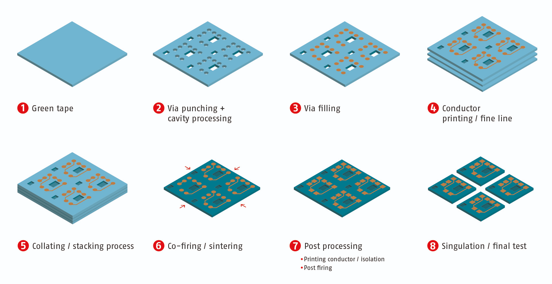
Actually, the manufacturing for HTCC Ceramic Substrate PCB is the same as LTCC Ceramic PCB, only the co-fired temperature is above 1500oC while LTCC should be sintered under 1000oC. Below are the fabrication steps for HTCC Ceramic PCB:
-
Green tap: For the production of HTCC we use prefabricated green foils. Cut the green foil into required size and shapes by laser cutting, then clean and polish it to remove any impurities or roughness on the surface. The substrate is typically made of aluminum oxide or aluminum nitride due to its excellent thermal conductivity.
-
Via punching and cavity process: Depending on the given design, punching and drilling via holes and cavities by laser machine, is done to create the necessary connections and paths for the circuitry. The laser beam is focused on the substrate surface, creating tiny holes that are typically around 50 microns in diameter. The holes are drilled according to the design specifications, which determine the number, size, and position of the holes.
-
Via filling: This is to fill some metal paste such as gold or silver to vertical contact in the multilayer structure. The metal pastes are then screen printed onto the green foil to form the planar electrical conductor paths. Due to HTCC technology are always in multi-layer structure, via hole creating and filling is very important.
-
Conductor printing: The conductor paste for HTCC generally is gold, silver, copper or Ag-Pd, which have high conductivity and are aimed to create the conductive pathways for the circuitry. Printing the conductor material onto the substrate evenly using a mesh screen. The screen is placed on top of the substrate, and the Ag paste is pushed through the mesh onto the substrate surface. The thickness of the printed layer is determined by the mesh size and the viscosity of the paste.
-
Collating/stacking process: Due to the HTCC ceramic printed circuit board are multi-layer PCB, once finishing the conductor printing process, it is needed to collating the layers and laminate them into one substrate, this is similar to the multi-layer FR4 PCB. The important thing during the collating process is that each layer much align with each other correctly, otherwise, it will cause defective boards or circuits can be connected with each other.
-
Sintering/co-firing: After the laminating process, the substrate is heated to a high temperature to sinter into a whole ceramic board. The sintering process typically takes place in a furnace at temperatures above 1500°C for several hours. During this process, the metal paste particles diffuse and bond with each other, forming a continuous and uniform layer.
-
E-Test: The next step is to perform an E-Test (Electrical Test) to ensure that the conductive pathways are working correctly and that there are no defects or shorts in the circuitry. The E-Test is carried out using a probe station and a testing device, which measure the electrical resistance and continuity of the circuitry. The E-Test can detect any defects or issues in the circuitry, such as open circuits, short circuits, or low resistance.
-
Surface Treatment: After the E-Test is completed, the substrate is treated with a surface treatment to protect the circuitry from damage and to improve its performance. This process involves applying a protective coating to the substrate, which can be either organic or inorganic. The surface treatment can improve the adhesion, wetting, and solderability of the circuitry, as well as protect it from environmental factors such as moisture, dust, and temperature fluctuations. Some common surface treatments include OSP, ENIG and ENEPIG.
-
Laser Cutting: Once the surface treatment is complete, the substrate is laser cut to create the final shape and size of the HTCC ceramic PCB. The laser cutting process involves using a laser beam to cut the substrate into the desired shape and size, according to the design specifications. The laser-cutting process is precise and accurate and can create intricate shapes and patterns. The laser beam melts and vaporizes the substrate material, creating a clean and precise cut.
-
Depanelization: De-panel the substrate into a single piece. Please make sure to de-panel the ceramic circuit board along the dividing line with a small plier, otherwise, the board will easily to get broken.
-
FQC: After the substrate has been cut, it undergoes a final quality check (FQC) to ensure that it meets the required specifications and standards. The FQC involves a visual inspection of the HTCC ceramic PCB, as well as electrical testing and functional testing. BSTCeramicPCB performs FQC and QA inspection processes to ensure the quality of product.
 Products
 About us
 Contact us


