


 HOME
HOMEManufacturing Processes Of Thick Film Ceramic PCB
Thick film ceramic PCB manufacturing steps
The utilization of ceramic PCBs is ubiquitous across a range of industries including but not limited to automotive electronics, communications, and aerospace, primarily due to their exceptional high-temperature resistance and insulation properties. The incorporation of thick film technology enhances the insulation performance and resistance accuracy of the circuit while also minimizing the impact of external factors such as temperature and humidity, resulting in superior adaptability to the external environment when compared to an independent soldering circuit. Given the numerous benefits associated with the thick film ceramic PCB, it's imperative to understand the fabrication process involved in its creation, and as such, here are some essential steps that one must follow.
Step 1: Raw Material Selection and Outline Cutting
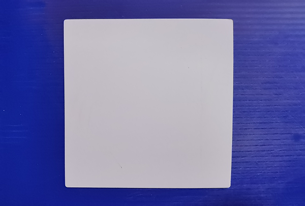
To initiate the production of thick film ceramic PCBs, the choice of raw material plays a vital role. Currently, three fundamental substrates are commonly employed - Aluminum Oxide (Al2O3), Aluminum Nitride (ALN), and BeO. The selection of the substrate depends on factors such as thermal conductivity, electrical insulation, and specific application requirements. For comprehensive details regarding thick film ceramic PCB raw materials, you can visit BSTCeramicPCB's Ceramic Substrate page. Notably, the standard size of a common ceramic substrate is 114x114mm, but the specifications should be checked according to BSTCeramicPCB's manufacturing capabilities.
Step 2: Substrate Drilling
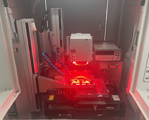
Once the raw material is ready, the designers proceed with the critical steps of substrate drilling and outline cutting. Advanced laser machines are employed for these tasks, offering precision and efficiency. The choice of laser technology varies depending on factors such as drill hole size, substrate dimensions, and surface smoothness. The most common laser types include cold light sources (UV light), carbon dioxide (CO2), and fiber cutting. To ensure the edges of the holes remain pristine during CO2 laser processing, a protective material layer is added to the ceramic substrate. Generally, operators will print a layer of red coating on the substrate surface, this is aim to avoid ceramic substrate reflection resulting in drill leakage.
|
|
|
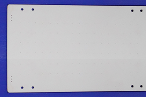
Step 3: Blackening Spot Removal after Laser Drilling
After the drilling process, it is essential to remove the protective material from the surface and thoroughly clean the holes. This preparation is crucial for the subsequent steps of copper spurring or conductive film printing. Failure to clean the residue adequately can adversely affect vacuum sputtering on the ceramic surface and hinder the adhesion of copper molecules or conductive materials in the holes. For thick-film circuits, this process may be more complex due to relatively large hole sizes.
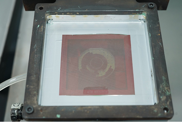
Step 4: Stencil Preparation
Simultaneously, the process of laser drilling/scribing and stencil-making commences. These tasks are typically assigned to different production workshops. The stencil, made from hard aluminum or aluminum alloy, is a vital component of thick film circuits. Stencil sizes typically measure 100mm x 150mm or 150mm x 200mm, featuring a rectangular outline. Foils for thick film circuits are generally constructed from stainless steel or nylon. Photosensitive glue is used to achieve a thick ink film for the trace, with a recommended optical film thickness of 20-30μm and no edge defects after development.
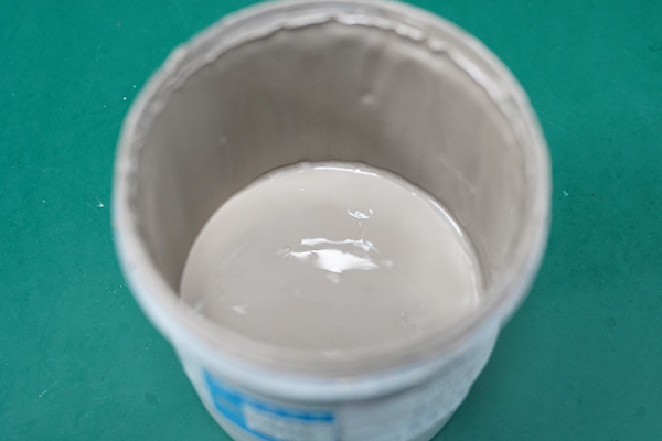
Step 5: Conductive Ink Preparation
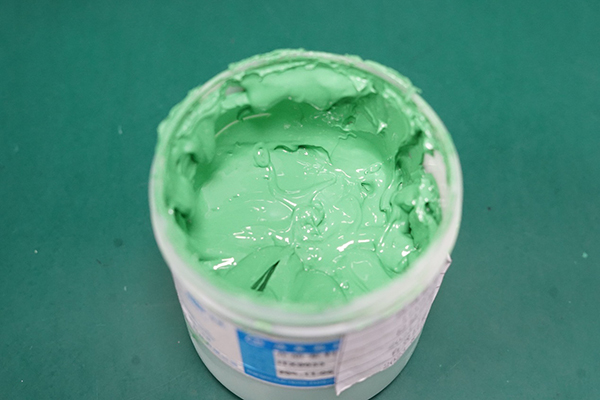
The next crucial step involves the preparation of conductive ink, a vital component of thick film ceramic PCBs. Different types of conductive ink are utilized for various applications, such as conductor ink, resistance ink, and insulating ink. These inks typically consist of noble metals and glass with low melting points. Gold, silver, platinum, palladium, and combinations like AgPd, AgPt, and Au are common choices for thick film circuits. The metal powder is dispersed in an organic resin binder, forming the conductive ink that is then applied to the ceramic substrate using the stencil. High-temperature firing burns off the organic resin binder, leaving behind pure noble metal, which bonds to the substrate due to the effect of the glass.
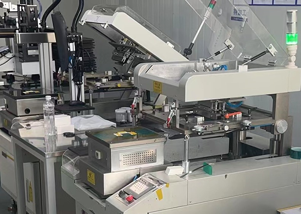
Step 6: Sample Making
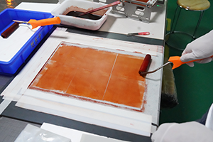
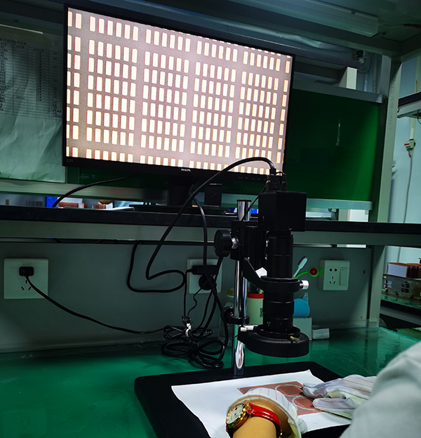
Sample making is a pivotal stage in the fabrication process. To begin, the ceramic substrate is securely fixed to a base by fixing the two adjacent sides. Air compressor-connected holes on the operating platform ensure the air between the substrate and the platform is removed, stabilizing the substrate. The stencil and substrate are accurately aligned, and the conductive ink is then applied to the substrate using a squeegee. The choice of squeegee material, like polyamine rubber or fluorinated rubber, and its hardness, typically A70° to A80, are carefully considered based on the circuit's pattern. Thick film integrated circuits employ three types of printing machines: manual, semi-automatic, and fully automatic. To ensure high-quality results, the product undergoes a thorough inspection using a 10-20 times microscope, where any trace opening or shorting issues can be easily identified.
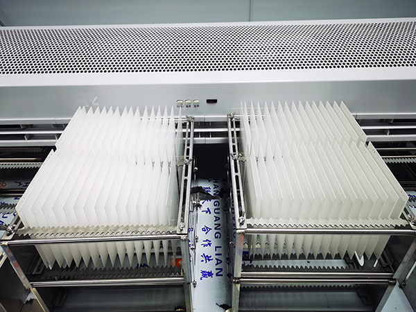
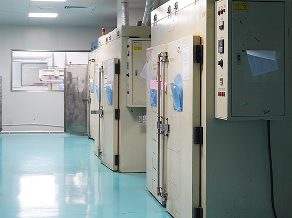
Step 7: Spreading, Drying, and Firing
Once the sample is prepared, the spreading, drying, and firing process begins. The product is left aside for 5 to 7 minutes after printing to allow the netted texture to disappear during the spreading phase. Drying is performed at around 100 degrees Celsius, and in cases where single-layer circuits without resistance need to be printed, baking ovens are utilized directly. Firing in the oven is crucial to combine the conductive ink with the ceramic substrate. As the firing oven reaches high temperatures, a tray with high-temperature-resistant material is employed.
Step 8: Printing Resistance Ink and Laser Resistor Trimming
Resistance ink is printed on the ceramic substrate after the conductor circuit is completed. Depending on the resistivity required, printing is carried out using the appropriate value ink. If multiple resistivities are needed, separate printings are carried out for each value. The resistors are dried after printing, but high-temperature firing is not required every time, only during the last printing session. Laser resistor trimming is employed to achieve precise resistance values. To customize this process according to the circuit, a jig board for adjusting the negative value is used, with probes fixed based on the resistor's position. Different boards necessitate distinct jigs for accurate trimming.
Step 9: Printing Glass Glaze for Protection
Printing glass glaze is the next step, a process similar to conductive ink printing. However, the firing temperature for glass glaze is lower than that for conductors, generally around 400-500 degrees Celsius. Glass glaze serves as a protective layer for ceramic PCBs, shielding them from oxidation, wrong soldering, and offering insulation properties. Similar to solder masks in PCBs and overlays in flexible circuit boards, glass glaze also acts as an insulated layer between traces. The glaze is available in two primary colors for thick film ceramic PCBs: blue and green.
Step 10: Finished Product Testing, Packing, and Shipment
The final step involves comprehensive testing to ensure the thick film ceramic PCBs meet the highest quality standards. After rigorous inspection, the PCBs are packed and ready for shipment. As a leading manufacturer of Ceramic PCBs in China, BSTCeramicPCB meticulously controls each manufacturing process to deliver high-quality ceramic boards precisely according to the customers' drawings.
For any inquiries or further information about Ceramic PCBs, feel free to contact BSTCeramicPCB or email sales@bestpcbs.com today.
 Products
 About us
 Contact us


