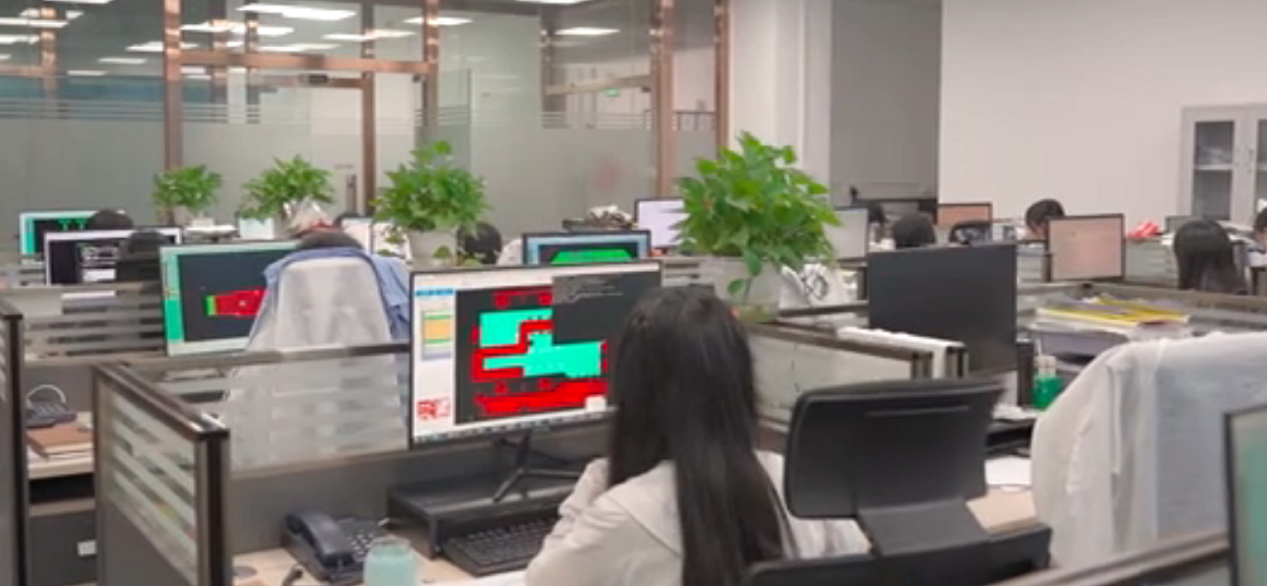
What's ceramic pcb design?
Ceramic PCB design is divided into Your Own PCB Design
and Design Your Own PCB according to customer purpose.
Your Own PCB Design is that Ceramic PCB factories or Ceramic Substrates companies produce in batches according to the original drawings the design drawings and materials sent by customers. Design Your Own PCB Design refers to the company's plan to provide customers with customized design and IC material selection after understanding the customer's application products and performance parameters.


-
Your Own PCB Design
When you have design information
When the customer has a designed PCB circuit diagram, BSTCeramicPCB will assist in the design guidance to ensure the perfection of the layout and save proofing and production costs. We play the role of a processing factory, covering an area of 3000㎡, with 200+ employees. Can independently produce FR4 PCB, Metal Core PCB, Ceramic PCB, Flexible Circuit and Rigid-flex PCB. The peak daily output is 100 square meters.
01
-
Design Your Own PCB
When we design your specified product Ceramic PCB
Many customers have new projects, but there is no PCB circuit design. Trying to operate with design software will miss many unreasonable points. BSTCeramicPCB has 17 years of experience in custom ceramic PCB design of industrial projects, tailor-made application circuit diagrams for customers, ensuring the rationality of performance and operation, and controlling the cost of mass production.
02
-
Ceramic PCB Layout
Relatively Simple
Compared with FR4 PCB, Metal Core PCB, Flexible Circuit and Rigid-flex PCB, the circuit layout of Ceramic PCB is relatively simple. Because the more complex the circuit on the ceramic substrate, the greater the consumption of conductive metal and the greater the cost.
03
-
Check Ceramic PCB Details
Engineers Team Check Again
Whether it is "design your own PCB" or "your own PCB design" customer, before proofing production, the business colleagues of BSTCeramicPCB will confirm with the customer the acceptable error value of some important data. For example line width, board thickness, conduct material, layers, silkscreen, glass glaze and conductive layer material, etc.
04
-
Mail Ceramic PCB Sample
Rapid Prototype And Test Again
After checking the value of the ceramic circuit board, BSTCeramicPCB's factory will make a proof. Mail it to the customer and put it into the project for testing. Of course, you can check the poor performance of the production process. When the customer is satisfied with our design and the degree of sample reduction is qualified, we can proceed to the mass production stage.
05
-
Put Into Production
Small Volume To Mass Production
After the customer confirms the ceramic PCB sample with BSTCeramicPCB, it can be put into the mass production process. The proofing cycle is generally within one week, and it takes 3-5 weeks from design, proofing to mass production.
06
-
01
Are you a PCB design software company? No, we are a manufacturer in China who focus on PCB manufacturing for 17 years. Have own 6 persons experienced engineering team.
-
02
Which industries have you designed ceramic substrate boards for? Aerospace, defense, communications, medical, automotive, laser equipment, etc.
-
03
How long will it take to design my project circuit layout? Common single-layer and double-layer ceramic substrates are completed within a week, and there are many variable factors in multi-layer, which will exceed a week.
-
04
Which metals can BSTCeramicPCB choose as conductor? Al2O3, BeO, Silicon Nitride, Copper, Golden, Platinum, etc.
-
05
What types of ceramic PCB can BSTCeramicPCB design? Thick Film Ceramic PCB, AMB Ceramic PCB, DPC Ceramic PCB, DBC Ceramic PCB, LTCC Ceramic PCB, HTCC Ceramic PCB.
-
06
What kind of formats of design files are acceptable? Gerber file, PCB, PCBDOC, BRD, CAM, CAD, ODB++(.tgz), ASC and DXF.


 HOME
HOME


