


 HOME
HOMEWhat is DBC Ceramic PCB?
What is DBC ceramic PCB?
A DBC ceramic PCB, full name is Direct Bonded Cooper ceramic boards, as its name implies, it is a technology process that bond the copper conductor on the ceramic substrate directly under appropriate temperature. For numerous years, DBC ceramic substrates have consistently demonstrated their effectiveness in providing outstanding solutions for the electrical isolation and thermal management requirements of high-power semiconductor modules.
The Structure of DBC Ceramic PCB
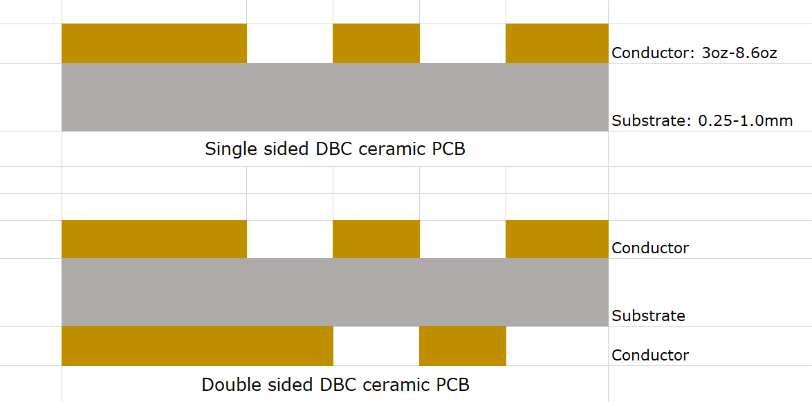
The main process of DBC ceramic PCB manufacturing
In fact, all the ceramic circuit boards feature a very good thermal conductivity and low CTE (coefficient thermal expansion) because the ceramic substrate itself has such properties. But ceramic board manufactured with different technology process has different advantages:
1. The thicker copper layer permits ceramic board has higher current loading for the same conductor width. Assuming the same copper cross-section the conductor needs to be only 12 % of that of a normal printed circuit board.
2. DCB ceramic PCB is gradually become the base materials of construction and interconnection technology of high-power semiconductor electronic circuits and also have been the basis for the "Chip-On-Board" (COB) technology which represent the packaging trend in the future.
3. Excellent electric insulation voltage means it can greatly improve the safety for the user.
4. Good thermal conductivity and heat-transfer provides the possibility of small packaging of the chips, result in increasing of power per unit of volume, improving reliability of systems and equipment.
5. The super-thin (0.25mm) DBC substrate can be an alternative material for beryllium oxide (BeO), it eliminates the unfriendly of environmental protection and toxicity; but seldom be used, as it is extreme expensive!
6. Superb thermal stability and power cycling capabilities (up to 50,000 cycles) makes it well-suited for applications that require in high temperature and high voltage environments, such as aerospace.
Where Can I Use the DBC ceramic PCB?
A: Insulated Gate Bipolar Transistor (IGBT chips)
B: Power supply for telecommunication
C: Power semiconductor modules
D: High frequency switch mode power supplies (SMPS)
E: Solar cell component
F: Automotive system
G: Aerospace
DBC Ceramic PCB Manufacturing Capability from BSTCeramicPCB
| Item | DCB/DBC Capabilities | |||||
|---|---|---|---|---|---|---|
|
Layer Count |
2 Layers |
|||||
|
Max Board Dimension |
138*178mm |
|||||
|
Min Board Thickness |
0.30mm.0.40mm |
|||||
|
Max Board Thickness |
1L: 1.3mm; 2L 1.6mm |
|||||
|
Conductor Thickness |
3.90Z-8.60z |
|||||
|
Min Line Width/Line Space |
12/12mil (0.30/0.30mm) |
|||||
|
Substrate Type |
AI203,ALN, Zro2 |
|||||
|
Substrate Thickness |
0.25, 0.38, 0.50, 0.635, 0.76,1.0mm |
|||||
|
Min Hole Diameter |
4mil (0.1mm) |
|||||
|
Min Hole Spacing |
NPTH: 16mil (0.30mm); PTH: 20mil (0.5mm) |
|||||
|
Min PAD Ring(Single) |
N/A |
|||||
|
PTH Wall Thickness |
N/A |
|||||
|
Min Solder PAD Dia |
8mil (0.20mm) |
|||||
|
Min Soldermask Bridge |
8mil(0.20mm) |
|||||
|
Min BAG PAD Margin |
8mil (0.20mm) |
|||||
|
PTH/NPTH Dia Tolerance |
PTH: ±4mil (0.1mm) ; NPTH: ±2mil (0.05mm) |
|||||
|
Hole Position Deviation |
± 4mil (0.1mm) |
|||||
|
Outline Tolerance |
Laser: +0.2/0.05mm |
|||||
|
Line Width/Spac Tolerance |
+5mil (0.125mm) |
|||||
|
Surface Treatment |
OSP/Ni Plating, ENIG |
|||||
|
Thermal Stress |
3 x 10 Sec @ 280C |
|||||
Choose BSTCeramicPCB, we can be your reliable supplier in China. Contact us right now to get your DBC ceramic solutions.
 Products
 About us
 Contact us


