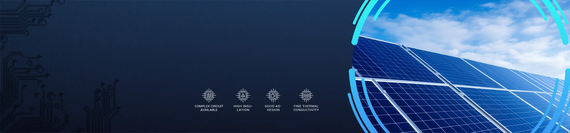
What's DPC Ceramic PCB (Substrates)?
DPC Ceramic PCB, also known as Direct Plated Copper Ceramic PCB, is a type of printed circuit board made from ceramic materials with a copper layer directly plated onto the ceramic substrate. Based on the thin film technology, the metallization of the ceramic surface can be achieved by magnetron sputtering, and the thickness of the copper layer is greater than 10 microns by electroplating. This technology offers several advantages compared to traditional copper-clad laminate PCBs.
Manufacturing Processes of DPC Ceramic PCB
DPC process in Ceramic PCB Manufacturing is a briefly critical process summarized in the chart below. Different from DBC or thick film ceramic PCB, using DPC technology we can achieve various patterns through the etching process. And a simple electrical characterization for DPC substrate is then utilized to extract the high-frequency dielectric constant and dissipation factor.
Here is a detailed description of each step:
1. Ceramic substrate
The substrate mainly used for DPC ceramic PCB are aluminum oxide (96% Al2O3 or 99.6% Al2O3) or aluminum nitride (ALN) without copper cladding. In general, the ceramic substrate is cut to the required single or array size using a laser.
2. Laser drilling
Laser drilling is used for hole drilling. due to the ceramic substrate being fragile and easy to be broken, the mechanical digital control (NC) drilling machine is not suitable for ceramic board. For boards that require a plated through hole (PTH), the holes are drilled through the substrate by laser, which can also be used via holes to electrically connect both sides of the ceramic substrate if needed. Non-plated through holes (NPTH) are also drilled with a laser.
3. Sputter
The sputter deposition technique is used for plating copper on both sides of the bare substrate, covering it with a copper layer. The sputtering process deposits a very thin copper film (generally 1um in thickness) on the ceramic substrate and in any pre-drilled holes, resulting in a ceramic-based copper-clad laminate (CCL).
4. Dry film – Exposure - Development
Apply a layer of dry film to the thin copper film on both sides of the copper-plated ceramic substrate, followed by exposure to UV lights through a photomask. The dry film is then developed by etching the polymerized part of the dry film through chemical or physical cleaning. This exposes some parts of the copper film, which form the required circuit patterns based on the Gerber artwork of the ceramic board, resulting in the required copper areas of a circuit board on the ceramic substrate. Copper features such as patterns and annular rings can be printed on the dry film.
5. Copper plating
Copper plating is done to fill the exposed parts of the dry film on the ceramic substrate with a suitable conductor (generally is copper) thickness and width, forming the copper features. The metalized circuit area has slender, flat, and smooth characteristics with good heat dissipation. If the plated copper thickness is thicker than required, extra copper is ground off using a high-end ceramic grinding machine, which has 1μm high precision per grinding cycle. The copper plating thickness is 1-3oz usually, when required thickness is more than 3oz, using DBC/DCB technology is the ideal choice.
6. Stripping
Strip refers to removing the remaining dry film on the ceramic board, and then you can see the circuit pattern that generated.
7. Etching
Etching the seed metal copper.
8. Surface treatment
The surface treatment for DPC ceramic board generally are OSP, ENIG and ENEPIG. Coating a layer of surface finishing prevents the oxidization of the conductor surface and improves the adhesion for the wire bonding. Different surface treatment has their unique benefits, for example, the ENEPIG is suitable for gold or alumina wire bonding, so if your ceramic board is designed to do bonding, ENEPIG is the ideal treatment.
The result is a high-quality, reliable Direct Plated Copper Ceramic PCB with excellent thermal and mechanical properties.
Characteristics of DPC Metallization Ceramic PCB
A DPC ceramic PCB features in excellent thermal and mechanical properties, which makes it is ideal for high-power applications where reliability and performance are critical. Below are some characteristics of this kind of ceramic board.
1. High thermal expansion and superior thermal conductivity
2. Versatility in widely various fields
3. Fine line width and space that enables to density of circuits
4. Outstanding high-frequency characteristics
5. Cost-effective and quick turnaround for prototypes makes
6. High-temperature resistance from -55oC to 850oC makes it well-suit in harsh environments
Applications for DPC ceramic PCB
Based on the substrate material use and manufacturing processes, the DPC metallization ceramic board provides good heat transfer and high mechanical performance in high-power fields, here are some typical applications listing as below:
1. High-power and high-current LEDs
2. Semiconductor modules such as IGBT
3. Cells for solar concentrators
4. Sensor in automotive motor control
5. High insulation & high voltage devices
6. Portable coolers
In addition, DPC substrates with excellent electrical performance can be considered for radio frequency (RF) applications or microwave components, which require a very low loss. These DPC substrates can therefore be widely used for high-frequency components that require high power and high heat.
As a professional manufacturer of Ceramic PCB in China, BSTCeramicPCB has more than 17 years experiences of Ceramic printed circuit board manufacturing, designing, layout, we believe we can be your best choice and reliable ceramic PCB vendor in China.


 HOME
HOME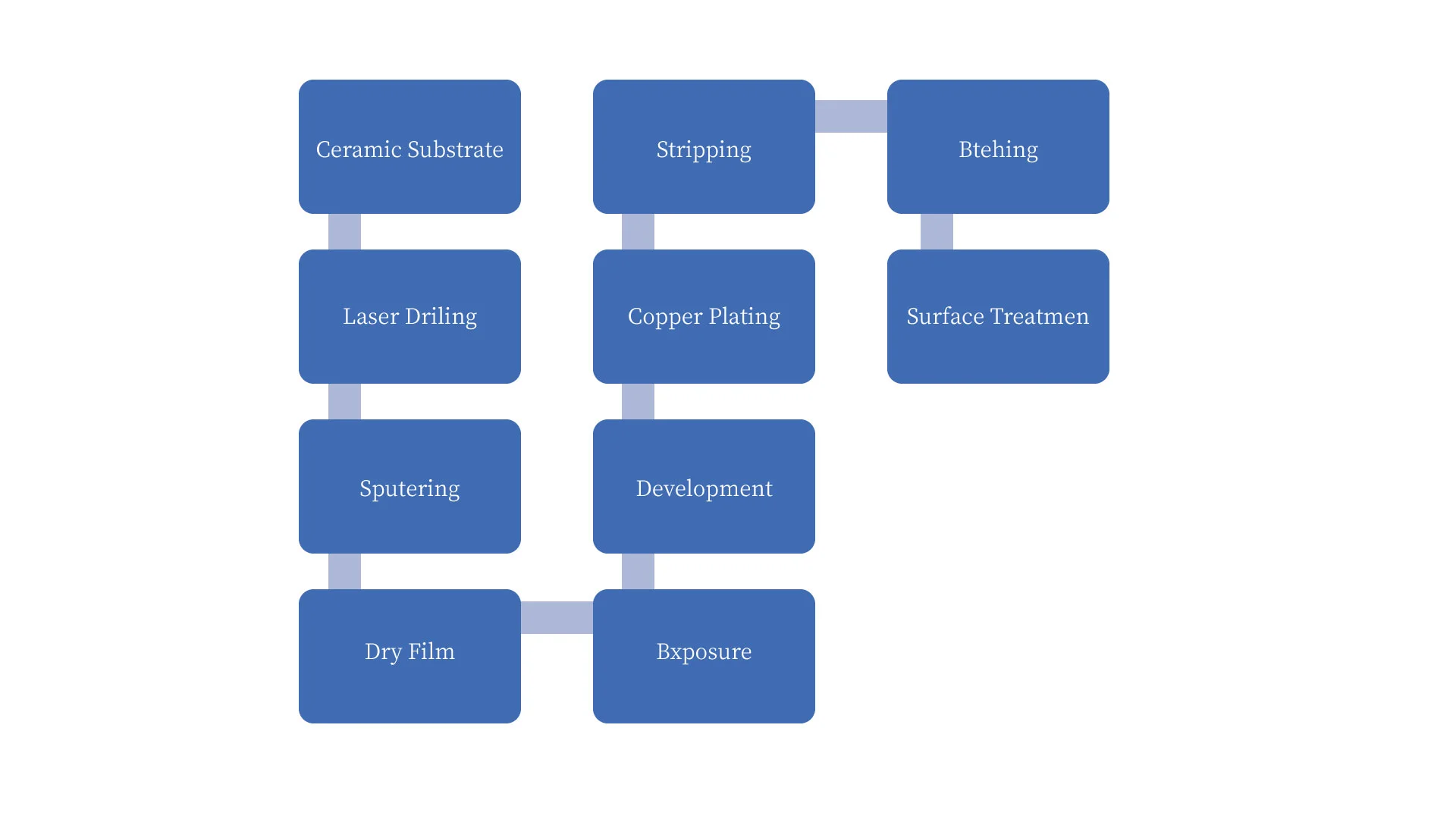
 Products
 About us
 Contact us


