


 HOME
HOMEYielding Processes Of AMB Ceramic PCB
AMB technology, a further development of DBC technology, is a method of using the active metal elements in the solder (e.g. Ti/Ag/Zr/Cu) to achieve the bonding of the ceramic to the metal. The ceramic forms a reactive layer that can be moistened by the liquid solder.
The bonding in the AMB ceramic substrate PCB is achieved through a chemical reaction at a temperature between the ceramic and the active metal filler metal, and the Si3N4 ceramic used in the AMB has higher thermal conductivity (>90W/mK 25℃) and is closer to the thermal expansion coefficient of silicon (2.6x10⁻⁶ /K) than the traditional AI2O3 ceramic substrate. As a result, the AMB substrate has high bonding strength and reliability. Combined with the silver sintering process and high-power silicon carbide chips, the AMB copper layer with the active metal coating enables high power, better heat dissipation and highly reliable packaged modules (able to withstand 3,000 thermal shocks) that have been widely used in electric vehicles, electric locomotives and high-speed trains.


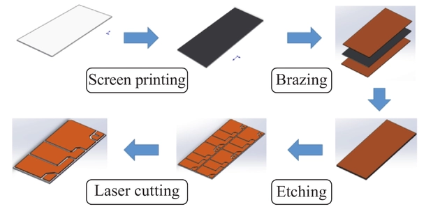
The main processes for AMB ceramic PCB are:
- Pre-treatment for copper foil and ceramic substrate
- Laminate the copper and substrate and then solder in high temperature vacuum furnace
- Chemically etch the copper on the ceramic surface and generate the patterns and circuits
- Laser cut the panel ceramic board into single piece
Different with DBC ceramic board, the copper on the AMB ceramic is brazed with the substrate through an extra screen print step, while the copper on DBC product is directly bonding on the substrate. Additionally, the copper for DBC products is formed by a single etching, while for AMB products with additional metal brazing layers, additional etching processes are required to remove the filler metal, usually with hydrofluoric acid. Below is the flow chart for a AMB ceramic board:
1. Raw material
The raw material for AMB is copper belt, ceramic substrate and extra special active metal elements.
Copper belt: in the current industry, the popular copper belt is Cu-OFE (include copper >99.99%, oxide<0.0005%). In normal situation, it was supplied in a belt, so we should laminate and cut into the required dimension before production.
Active metal element is a mixed paste material with a certain adhesion. It is usually store in sub-zero (<0oC) to ensure the good performance, and should be thawed and mixed immediately before use.
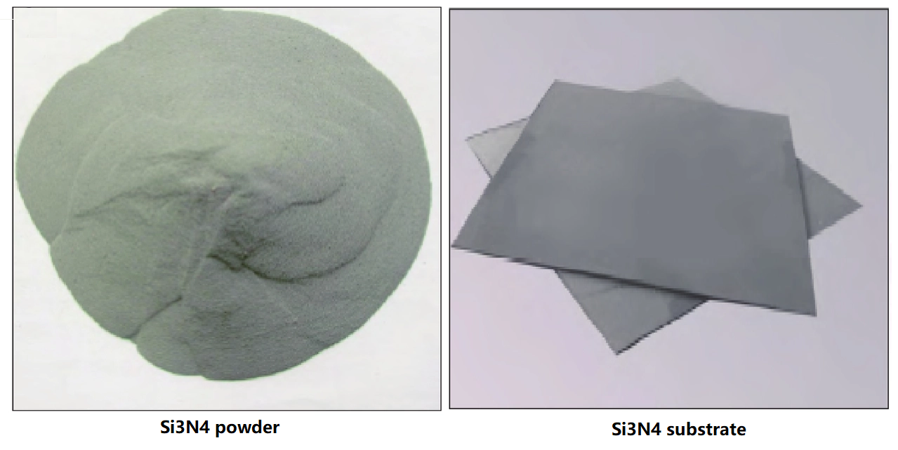
Ceramic substrate for AMB technology is Si3N4, which has higher thermal conductivity. The Si3N4 is generally supplied in powder, after a series of mixing, printing, molding process, we can get a substrate that need for AMB.
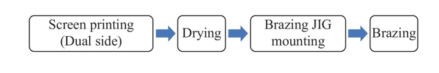
2. Screen printing
Take out the active metal element and stay indoor temperature to make sure the adhesive and properties of the metal are before screen printing. Next, stir the metal by a centrifugal stirrer, this step is to remove the bubbles in the solder, ensure the solvent is fully mixed with the active metal.
In order to ensure that there is enough solder on the surface of the ceramic sheet after printing, the ceramic sheet should be weighed before and after printing for a comparison. If the printing thickness is abnormal, alcohol can be used to scrub the solder on the surface and then printing again.
3. Brazing
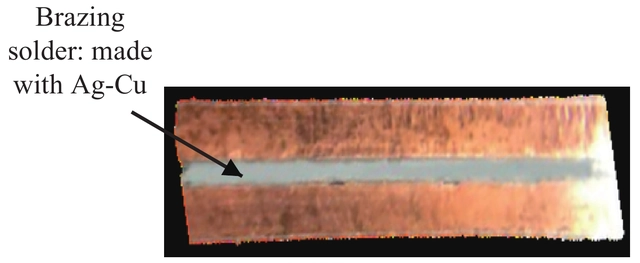
In this step, active metal solder will be used for brazing the copper and ceramic substrate. The brazing solder (which includes Ti/Ag/Cu elements) will react with ceramic, creating a reactive layer that can be wetted by the liquid solder, thus achieving the mount of metal on the JIG without the metallized ceramic. Below is a flow chart of this process that will make you sense.
From the below picture, we can see the brazing solder is in the copper and ceramic.
Bubble is a key defect of the AMB brazing process. Therefore, ultrasonic scans are introduced after the brazing process to detect bubbles beneath the copper created during the process. The hidden bubbles can affect the overall heat dissipation of the semiconductor module, resulting in reliability risks. To avoid such a problem, we will perform an ultrasonic scanning thermal shock after 3000 tests, to check whether there is stratification or bubbles between the copper and the ceramic.
4. Conducting film sticking and etch
The laminate and etching process is similar to the DPC ceramic PCB, below is a detailed flow chart for this process.
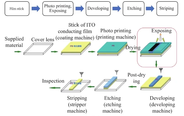
(Laminate-etching process)
5. 2nd etching
Due to there is a layer soldering in the ceramic, it is needed to repeat the etching process. However, it is better to use hydrofluoric etching acid to make sure the circuits on the AMB surface meet the electrical performance requirements.
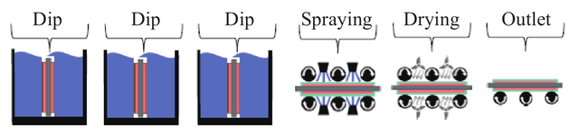
6. Electroplating
Before plating, clean the surface of the substrate to get a good plating. Then clean again with an acid to remove the oxide left on the surface. After that, the substrate is etched and immersed in the plating solution to complete the electronic plating.
The plating thickness needs to be monitored strictly, in general, we use XRF to measure the thickness of the plating and monitor the CPK. Below is the process of electroplating.
7. Laser cutting
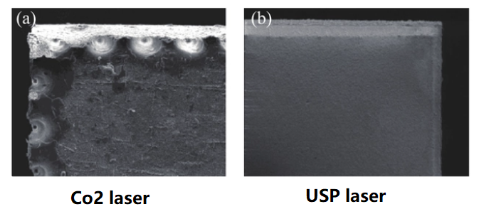
The laser cutting is cut the ceramic substrate according to the cross line to finish a pre-cutting. In this process, there are mainly used Co2 laser machine or USP laser. Compared to Co2 laser, USP has less damage to the saw cutting path on ceramic, and the cutting surface forming effect is better. Due to its positive advantages, USP laser cutting is currently replacing CO2 laser in some domestic plants, and may be expanded to overseas suppliers.
8. De-panel
The AMB ceramic after laser cutting is still in panel, so we need to de-panel it into single piece according the cutting line. After de-panel, check and inspect the quality of circuit board to make sure defective-free products when deliver to customer.
AMB technology, a further development of DBC technology, is a method of using the active metal elements in the solder (e.g. Ti/Ag/Zr/Cu) to achieve the bonding of the ceramic to the metal. The ceramic forms a reactive layer that can be moistened by the liquid solder.
If you want to rapidly prototype or design an AMB ceramic PCB right now, please mail to sales@bstceramicpcb.com for more information.
 Products
 About us
 Contact us


