


 HOME
HOME


"Thick film PCB" refers to the thickness of the conductor layer on the ceramic PCB. Under normal circumstances, its thickness will be at least more than 10 microns (um), about 10~13um, which is thicker than the sputtering technology of thin-film ceramic PCBs, and of course, the thickness is smaller than DCB/DBC ceramic boards or FR4 boards.
Ceramic boards using thick film technology, through the manufacturing steps of printing and high-temperature sintering, resistors, capacitors, conductors, semiconductors, exchangeable conductors, etc. can be placed on the ceramic board. At the same time, using the thick film process, we can make all the resistors on the board have the same value, or set different values for different resistors on the same board.
-
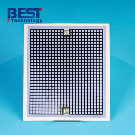
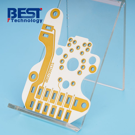
Thick Film Ceramic PCB For Ozonator
-
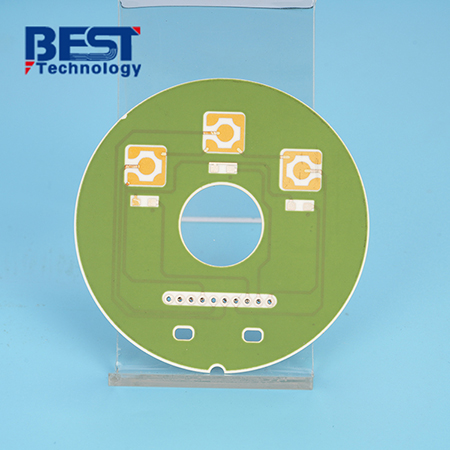
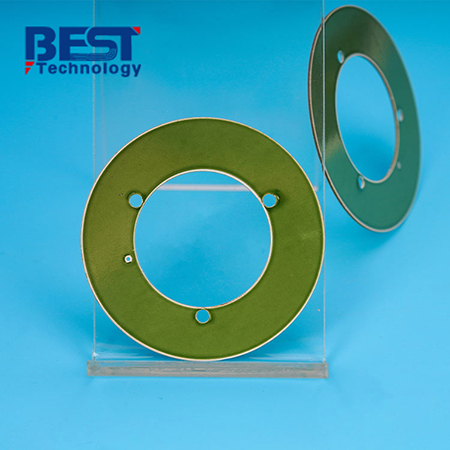
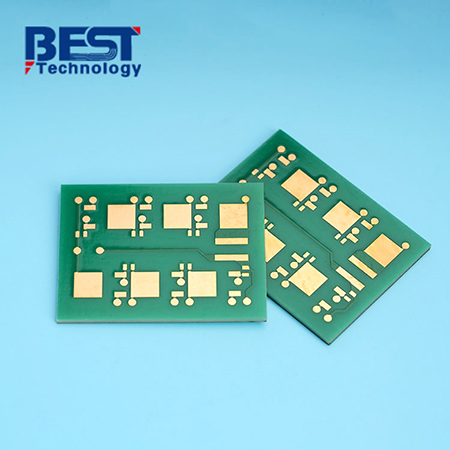
Thick Film Ceramic Substrate Board For Communication
-
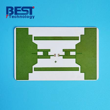
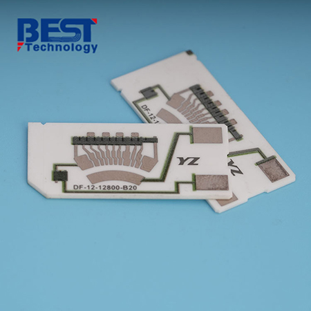
Al2O3 Thick Film Ceramic Substrate PCB For Medical Equipment
-
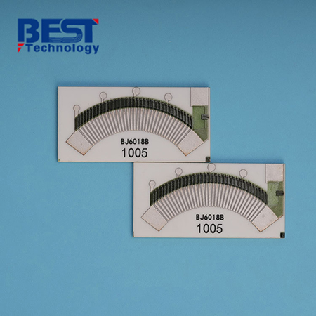
96% Al2O3 Thick Film Ceramic Substrate PCB For Defense
-
Thick Film Ceramic Substrate Double-side Circuit Board For Aerospace
-
Thick Film Ceramic PCB For Scientific Research And Education Machine
-
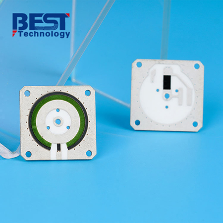
Thick Film Ceramic Substate PCB For Automotive Oil Level Sensor
-
Thick Film Ceramic Substrates PCB For Auto Fuel Gauge
-
BeO Thick Film Ceramic Substrate PCB For Laser Equipment
 Products
 About us
 Contact us


