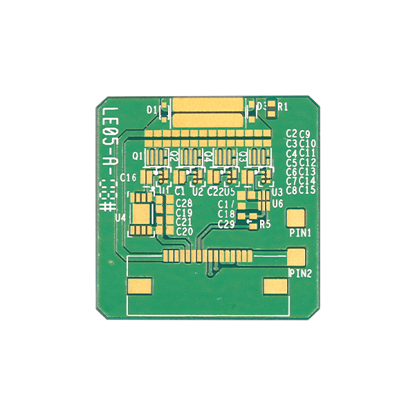
Which Process Ceramic Circuit Board Is A Better Solution For Semiconductor Refrigerator Chips?
With global warming, there are more and more commercial buildings, public spaces, and large-scale residences. Driven by the above two factors, the HVAC and refrigeration industry is developing rapidly, and people have higher and higher requirements for central air-conditioning and refrigeration systems. However, a major challenge faced by these industries is the insufficient cooling conditions of the refrigeration unit, especially the heat dissipation chip. Traditional heat sinks can easily overheat, causing performance issues and shortened lifespan of the heat sink. Solving this heat dissipation bottleneck has become a technological breakthrough in the industry.
To address this challenge, the use of ceramic PCBs has become a game changer in the refrigeration industry. In this article, we will explore the advantages and applications of ceramic PCBs in semiconductor refrigerators.
Five Ceramic PCBs: Comparison of Advantages

1. Thick film printed ceramic circuit board (TPC)
Thick film ceramic circuit boards are produced using traditional screen-printing technology to print metal wiring layers. Its manufacturing is relatively easy, the cost is relatively low, the production quality is relatively stable, and the reliability is relatively high. However, due to the limitations of the screen-printing process, TPC boards cannot obtain high-precision circuits. In addition, in order to reduce the sintering temperature and improve the bonding strength between the metal layer and the ceramic substrate, a small amount of glass phase is usually added to the metal slurry, which will inevitably reduce the Electrical and thermal conductivity of metal wiring layers. Making them less suitable for smaller and smaller heat sink chips.
2. Thin film ceramic circuit board (TFC)
Thin film ceramic circuit boards overcome some of the problems associated with thick film processes. TFC circuit boards use thin film processes such as magnetron sputtering, vacuum evaporation, and electrochemical deposition to form a metal layer on the surface of a ceramic substrate, and then form a specific metal pattern through processes such as masking and etching. This process has low operating temperature, high wiring precision, controllable metal layer thickness, and high bonding strength between metal and ceramics. Ceramic substrate materials commonly used in thin film processes mainly include Al2O3, AlN, and BeO. Thin film ceramic circuit boards are mainly used in device packaging with small currents, small sizes, high heat dissipation requirements, and high wiring precision requirements. Of course, it is suitable for small refrigeration chips that have high requirements on board thickness, weight, and volume.
3. Direct electroplated copper ceramic circuit board (DPC)
The DPC ceramic substrate uses a laser to drill holes in the ceramic substrate, uses a semiconductor process to deposit a Cu seed layer on the ceramic substrate, fills the holes through an electroplating process, and thickens the metal layer. This process has the characteristics of high circuit precision and low preparation temperature. This process enables vertical interconnection of ceramic substrates to increase packaging density. The disadvantage is that the metal circuit layer is prepared by an electroplating process, which pollutes the environment, the plating growth rate is low, and the thickness of the circuit layer is limited, making it difficult to meet the packaging needs of high-current power devices. DPC ceramic substrates are mainly used in high-power LED packaging.
4. Directly bonded copper ceramic circuit board (DBC)
DBC ceramic substrate is heated in oxygen-containing nitrogen at high temperatures above 1000°C, so that the copper foil and ceramic substrate are firmly bonded together through eutectic bonding. The bonding strength is high and the thermal conductivity is good. and thermal stability. It is widely used in packaging heat dissipation of insulated bipolar diodes, lasers, focused photovoltaics and other devices.
5. High-temperature co-fired ceramic circuit board (HTCC)
HTCC circuit boards use screen printing metal paste to fill wiring holes, and finally, the green layers are superimposed and placed in a high-temperature furnace for sintering. The process temperature is high and the selection of conductive metals is limited. Only metals with high melting points but poor conductivity can be used, and the production cost is high. Limited by the screen-printing process, the circuit accuracy is poor and it is difficult to meet the high-precision packaging requirements. However, the HTCC substrate has high mechanical strength and thermal conductivity, stable physical and chemical properties, and is suitable for device packaging in high-power and high-temperature environments.
6. Low-temperature co-fired multi-layer ceramics (LTCC)
Low-temperature co-fired multi-layer ceramics (LTCC): Similar to the HTCC preparation process, LTCC technology uses low-temperature firing to integrate multi-layer ceramic materials. At the same time, using metal pastes such as Cu, Ag, and Au with good conductivity, the LTCC substrate preparation temperature is low, but the production efficiency is high, and it can adapt to high temperature, high humidity, and high current application requirements. This technology is widely used in military and aerospace electronic devices.
Conclusion
To sum up, different processes have different advantages, disadvantages, and scope of application. Through the comparison of advantages, we can see that the common process options for manufacturing refrigeration chips are DBC and DPC.
DBC and DPC ceramic circuit boards have unparalleled advantages. Their excellent thermal conductivity and material properties meet the evolving requirements of the refrigeration industry, making them a catalyst for the continuous advancement of high-power refrigeration units.
Best Technology has extensive experiences in ceramic PCB manufacturing, if you are interested in it, welcome to call us or e-mail us at sales@bstceramicpcb.com.sales@bstceramicpcb.com


 HOME
HOME


